Report Overview
Chemical Mechanical Polishing Market Size:
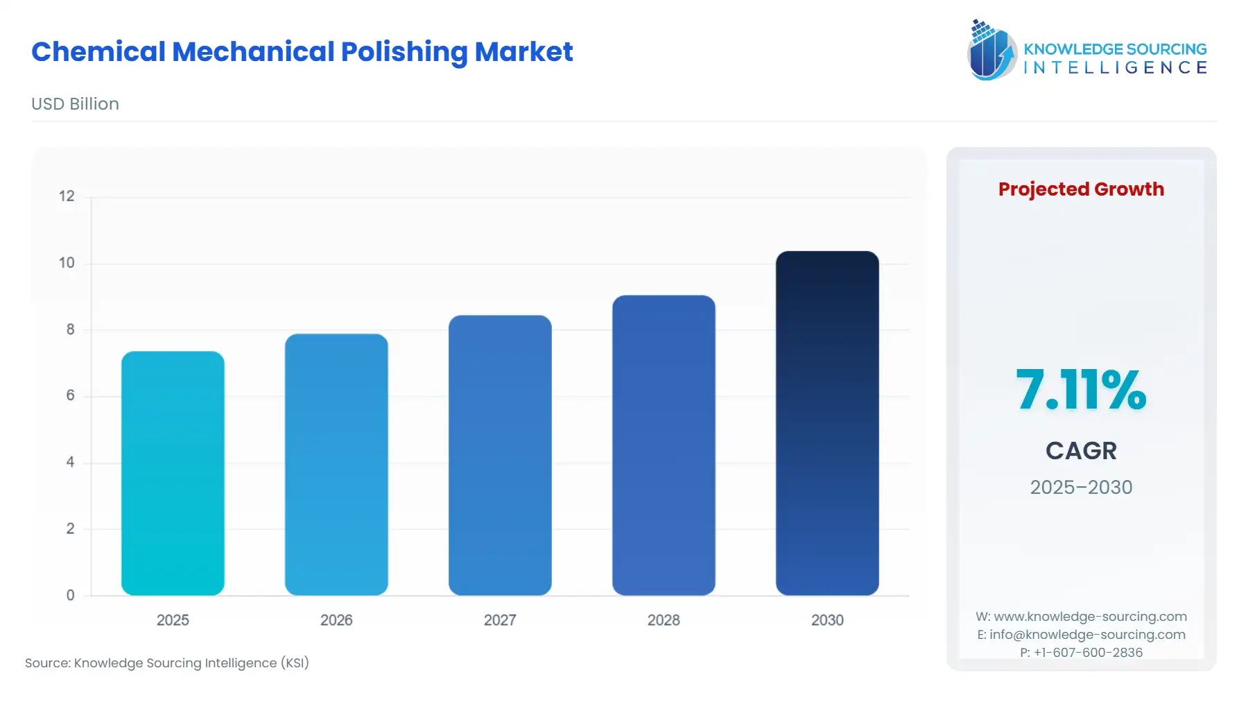
The chemical mechanical polishing market is forecasted to rise at a 7.11% CAGR, reaching USD 10.381 billion by 2030 from USD 7.365 billion in 2025.
Highlights:
- 1Advanced Node Complexity Drives Multi-Step DemandThe pervasive transition to smaller feature sizes, including 3nm and 2nm Gate-All-Around (GAA) transistor architectures, necessitates a significant increase in the number of planarization steps per wafer. This structural shift directly amplifies the demand for both high-precision CMP Equipment and specialised CMP Consumables capable of managing complex, selective material removal.
- 2Heterogeneous Integration Creates New Planarization ImperativesThe industry's reliance on advanced packaging technologies, such as through-silicon vias (TSVs) and hybrid bonding, requires ultra-flat surfaces for wafer-to-wafer or die-to-wafer stacking. This move into three-dimensional integration fundamentally expands the application scope and demand for CMP beyond front-end fabrication into the high-growth advanced packaging segment.
- 3Supply Chain Localisation Stimulates Regional Equipment PurchasesGovernment initiatives, particularly the U.S. CHIPS and Science Act, incentivise the establishment of new, domestic fabrication facilities (fabs) for advanced semiconductor manufacturing. This geopolitical trend directly catalyses a localised surge in capital expenditure for CMP Equipment within North America and Europe to build self-sufficient production capacity.
- 4Consumables, Define Process Yield and Cost of OwnershipThe recurring cost and technical performance of CMP Consumables (slurries and pads) critically dictate a Foundry's overall yield and operational expenditure. Innovations in tailored slurry formulations for new materials (e.g., Ruthenium and Cobalt) and advanced polishing pad designs are mandatory for sub-7nm fabrication, driving continuous demand for next-generation consumables.
Chemical Mechanical Polishing (CMP) constitutes a non-negotiable process within modern semiconductor manufacturing, serving as the bridge between traditional chemical etching and mechanical abrasion to achieve the near-perfect surface planarity essential for multi-layer device construction. Without this precise planarization capability, subsequent lithography and deposition steps fail, rendering the intricate three-dimensional structures of contemporary microchips—such as FinFET and, more recently, GAA transistors—impossible to realise.
The market fundamentally revolves around two interdependent segments: capital-intensive CMP Equipment and the high-volume, recurring revenue stream of proprietary CMP Consumables (slurries and pads). As Moore's Law continues to drive miniaturisation, the role of CMP has evolved from a simple levelling task to a high-precision, multi-step process for various materials, including dielectrics, metals (Copper, Tungsten), and emerging semiconductors. Market dynamics are governed by the massive capital expenditure cycles of Semiconductor Manufacturers and Foundries and the relentless technical requirements for tighter tolerances, lower defectivity, and increasing process selectivity at advanced nodes.
Chemical Mechanical Polishing Market Analysis:
- Growth Drivers
The most significant driver is the escalating number of CMP steps per wafer at advanced technology nodes (7nm and below). The structural complexity of Gate-All-Around (GAA) transistors and 3D NAND flash memory necessitates multiple planarization passes, which directly multiplies the demand frequency for both CMP Equipment utilisation and CMP Consumables replacement. Furthermore, the global shift toward advanced semiconductor packaging (e.g., 3D ICs, TSVs, and hybrid bonding) extends the application of CMP from front-end to back-end processes, creating a new, high-precision demand segment in Integrated Circuits (ICs) manufacturing. The geopolitical imperative for supply chain resilience, highlighted by the U.S. CHIPS Act, compels IDMs and Foundries to build new domestic fabs, resulting in a large, immediate, and localised capital expenditure demand for high-throughput CMP tools globally, counterbalancing the impact of US tariffs on global procurement decisions.
- Challenges and Opportunities
The primary challenge lies in achieving ultra-low defectivity and high uniformity across 300mm wafers for advanced nodes. Any defect resulting from the CMP process translates directly into yield loss, which is particularly costly for complex chips. This technical hurdle constrains the adoption of new materials and processes until validated. A major opportunity is the development of specialised slurries for emerging materials like Ruthenium and Cobalt used in advanced interconnects. As traditional Copper planarization faces limitations, the need for selective, high-performance slurries for these alternatives creates a high-margin demand opening for CMP Consumables suppliers. Another opportunity is the integration of real-time endpoint detection and AI-driven process control. Implementing advanced metrology and machine learning in CMP tools addresses the precision constraint, increasing demand for highly sophisticated, integrated CMP Equipment and associated Software.
- Raw Material and Pricing Analysis
The CMP market, being a physical product market, is highly dependent on the raw materials used in its Consumables. CMP Slurries are based on abrasive particles (e.g., colloidal silica, ceria, alumina, and diamonds) suspended in a chemical solution. The pricing of slurries is critically sensitive to the cost and supply chain stability of high-purity nano-abrasives and specialised chemical precursors. A key material, cerium oxide (ceria), often used in high-selectivity oxide polishing, can experience price volatility linked to rare earth element supply chains. CMP Pads, typically made of polyurethane, rely on stable polymer feedstock pricing. The industry follows a "razor-and-blade" model: CMP Equipment is a high-capital expense with a long lifecycle, while Consumables represent a high-volume, recurring operating expenditure. End-users (Foundries) exert constant pressure to reduce the cost-of-ownership (CoO), driving demand for longer-lasting pads and more efficient, higher-selectivity slurries that reduce material waste and CMP steps.
- Supply Chain Analysis
The global CMP supply chain exhibits a significant concentration in both equipment and consumables. CMP Equipment is primarily sourced from North America (Applied Materials) and Asia-Pacific (Ebara Corporation, Accretech), establishing these regions as major production hubs. The CMP Consumables segment is dominated by a few global chemical and materials science companies (e.g., DuPont, Fujimi, Entegris). Logistical complexities stem from the high-purity requirements for raw materials and the often short shelf-life and specific storage conditions required for advanced slurries, which necessitate tightly controlled, regionalised distribution networks. A key dependency is the direct, long-term technical collaboration required between equipment manufacturers, slurry/pad suppliers, and end-user Foundries to co-optimise performance for new device nodes. Any disruption in the supply of ultra-high-purity raw chemicals can immediately constrain the production capacity of advanced CMP Consumables globally, thereby impacting the entire semiconductor fabrication industry.
- Government Regulations
Regulations primarily focus on environmental standards, worker safety, and, increasingly, geopolitical strategy to secure domestic supply.
|
Jurisdiction |
Key Regulation / Agency |
Market Impact Analysis |
|
United States |
CHIPS and Science Act (2022) |
The Act provides massive financial incentives for building new domestic semiconductor fabs. This government policy acts as a direct and powerful catalyst for capital expenditure, generating non-discretionary demand for new, advanced CMP Equipment within the U.S. and among U.S.-aligned IDMs and Foundries. It simultaneously imposes restrictions on funding recipients' expansion in foreign countries, thereby geographically re-orienting future demand toward domestic suppliers. |
|
Europe |
European Union REACH Regulation |
REACH (Registration, Evaluation, Authorisation and Restriction of Chemicals) mandates rigorous substance testing and documentation for chemicals used in CMP Slurries and CMP Pads. This creates a significant compliance hurdle for suppliers, indirectly increasing R&D cost and driving demand for REACH-compliant and environmentally-friendly slurry and pad formulations to ensure market access across EU member states. |
|
South Korea/Taiwan |
Local Environmental Protection Laws |
Stricter wastewater discharge and waste management regulations in major fabrication centers (e.g., Korea, Taiwan) dictate how spent CMP Slurry must be treated or recycled. These regulations increase the operational cost for Foundries and IDMs, simultaneously creating a demand opportunity for equipment and Consumables suppliers that offer closed-loop, slurry recycling, or high-efficiency process solutions to minimize waste volume. |
Chemical Mechanical Polishing Market Segment Analysis:
- By Type: CMP Consumables
The CMP Consumables segment, encompassing slurries, pads, and conditioning discs, is the market's high-frequency, recurring revenue engine, fundamentally linked to wafer starts and process steps. The core demand driver is the necessity of precise material selectivity and defect control at shrinking technology nodes. As Integrated Circuits (ICs) move to GAA structures and advanced memory (3D NAND), each new layer requires a dedicated, chemically-engineered slurry and a specifically textured pad to polish one material (e.g., Copper) while minimising the removal of the underlying or adjacent material (e.g., low-$k$ dielectric). This high-selectivity requirement forces continuous, application-specific demand for novel slurry chemistries (e.g., ceria for dielectrics, alumina for tungsten, colloidal silica for shallow trench isolation). The consumption rate is directly proportional to fab utilisation rates; thus, periods of high global semiconductor Foundry output translate immediately into a surge in demand for Consumables. Furthermore, the rise of advanced packaging, requiring planarization of temporary bonding materials and TSVs, introduces new, high-purity Consumable demand streams outside the traditional front-end fabrication process.
- By End User: Foundries
Foundries (Pureplay and Contract Manufacturers) represent the largest and most critical end-user segment for the CMP market, with demand driven entirely by their mission to produce chips for diverse clients at the leading edge of technology. The primary demand driver is the relentless need for process control and yield maximisation across multiple technology nodes. Foundries operate complex, multi-client fabrication facilities, demanding highly versatile and reliable CMP Equipment that can quickly switch between different planarization processes (e.g., Copper, Tungsten, STI) with minimal downtime and zero cross-contamination. Their immense volume production creates massive, sustained demand for high-throughput CMP Equipment (primarily 300mm tools) and necessitates long-term, direct procurement agreements for high volumes of CMP Consumables. Furthermore, as the first adopters of new device architectures (e.g., 2nm GAA), Foundries exert significant demand pull on equipment and slurry manufacturers to rapidly co-develop and qualify next-generation polishing technologies, making them the technical demand catalyst for all market innovation.
Chemical Mechanical Polishing Market Geographical Analysis:
- US Market Analysis (North America)
The U.S. market is experiencing a profound demand transformation, driven almost entirely by the CHIPS and Science Act. This legislation has directly triggered multi-billion dollar announcements from major IDMs and Foundries to construct next-generation fabrication plants domestically. This strategic investment generates a massive, near-term capital expenditure demand for high-end CMP Equipment, specialised metrology, and high-purity Consumable manufacturing capability to support these new fabs. Local factors, including strong university research partnerships and a concentration of major CMP Equipment manufacturers (e.g., Applied Materials), facilitate co-development of new planarization techniques, further driving demand for leading-edge, domestically supplied technology.
- Brazil Market Analysis (South America)
The Brazilian CMP market is nascent, driven by regional demand for micro-electromechanical systems (MEMS) and specialised packaging, rather than leading-edge IC fabrication. Local factors constraining demand for high-end CMP tools include the absence of large-scale, advanced Foundries and the high cost associated with importing sophisticated machinery and proprietary CMP Consumables. Demand is primarily sustained by smaller, localised operations focused on mature-node semiconductor assembly and testing. Any significant future demand catalyst would require government-backed industrial policy or substantial private investment to establish a full-scale fabrication ecosystem.
- Germany Market Analysis (Europe)
The German market is centred on specialised manufacturing, including power electronics (Silicon Carbide, Gallium Nitride) and advanced automotive Micro-electromechanical systems (MEMS) fabrication. Local demand is characterised by a strong emphasis on precision, quality control, and automation. The stringent requirements of the automotive sector for zero-defect production drive specific demand for high-reliability, low-defect CMP systems and Consumables tailored for compound semiconductors, which require different planarization techniques than standard silicon. Furthermore, German manufacturers often prioritise CMP Equipment from vendors that demonstrate strong compliance with the EU's environmental and chemical regulations (REACH).
- Saudi Arabia Market Analysis (Middle East & Africa)
The CMP market in Saudi Arabia is currently characterised by low overall volume, with limited domestic Integrated Circuits (ICs) manufacturing. The primary demand stream is driven by recent government-led initiatives to diversify the economy through technology investment, creating initial demand for establishing basic semiconductor fabrication and research infrastructure. Procurement is highly concentrated on a few large-scale, strategic projects, focusing on acquiring baseline CMP Equipment for educational or initial pilot-scale production, often sourced through government tenders that favour comprehensive training and long-term service agreements from global OEMs.
- China Market Analysis (Asia-Pacific)
China is the world's single largest consumer of semiconductor materials, creating massive volume demand for both CMP Equipment and Consumables. Local demand is uniquely driven by a national strategy to achieve semiconductor self-sufficiency, backed by substantial state funding (e.g., the National IC Investment Fund). This policy propels demand for both large volumes of high-throughput 300mm CMP tools for new Foundries and IDMs, and crucially, creates intense demand for the rapid development and market qualification of domestically produced CMP Consumables (slurries and pads) to replace imports. The competitive environment is shaped by both a massive volume requirement and a national preference for local substitution, creating a dual-market structure.
Chemical Mechanical Polishing Market Competitive Environment and Analysis:
The Chemical Mechanical Polishing market exhibits a clear bifurcation: a highly concentrated CMP Equipment segment dominated by a few global technology leaders, and a moderately concentrated CMP Consumables segment defined by materials science expertise and proprietary chemical formulations.
- Applied Materials Inc.
Applied Materials is the indisputable market leader in CMP Equipment, leveraging its extensive Reflexion and OptiPlan family of polishers. The company’s strategic positioning centres on offering integrated materials solutions, combining equipment, process knowledge, and advanced metrology into a cohesive, high-yield system. Applied Materials capitalises on the complexity of advanced nodes by developing new CMP platforms, such as its solutions for 3D architecture, which secures non-discretionary demand from Foundries and IDMs engaged in cutting-edge logic and memory production. Its key competitive advantage is the deep integration of its CMP tools with other core semiconductor processes (PVD, CVD, Etch), making it a preferred partner for new fab build-outs.
- Ebara Corporation
Ebara Corporation maintains a strong competitive position in CMP Equipment, particularly within the high-volume, performance-driven Asia-Pacific region. The company’s strategic focus is on delivering high-throughput and low-cost-of-ownership polishing systems that appeal directly to high-volume Foundries. Ebara’s competitive differentiation often lies in its development of single-wafer cleaning and processing capabilities integrated with its CMP tools, addressing the critical issue of defect control. This specialisation in production efficiency and reliability ensures sustained demand from major Asian Foundries operating at maximum capacity, especially for established high-volume applications like memory device manufacturing.
- DuPont de Nemours Inc.
DuPont (or its subsidiary Qnity, depending on recent divisional structuring) is a foundational player in CMP Consumables, particularly dominating the CMP Pad segment with its IC1000 and newer Ikonic™ product lines. Its strategic position is defined by materials science leadership and established, long-term supply relationships with virtually all major Semiconductor Manufacturers. DuPont’s competitive strength is its ability to co-develop proprietary pad formulations that meet the extremely high selectivity, uniformity, and lifetime requirements of new process layers, thereby establishing itself as a mandatory supplier for advanced-node Foundries. The continuous innovation in their Ikonic™ pad platform, targeting new CMP applications, directly drives and captures demand created by the industry's progression to smaller nodes and exotic materials.
Chemical Mechanical Polishing Market Developments:
- October 2025: Applied Materials Unveils New Chipmaking Products to Supercharge AI Performance
Applied Materials, Inc. introduced new semiconductor manufacturing systems engineered to boost the performance of advanced logic and memory chips foundational to AI computing. While the press release focuses heavily on the Kinex™ Bonding system for die-to-wafer hybrid bonding and the Centura™ Xtera™ Epi System for Gate-All-Around (GAA) transistors, these innovations directly increase the upstream demand for ultra-precise planarization. Specifically, advanced packaging like hybrid bonding requires perfection in surface flatness, propelling demand for Applied's most advanced CMP Equipment to prepare the wafers for this critical stacking process.
- March 2025: DuPont Showcases Advanced Circuit Materials for AI-Driven Substrates
DuPont showcased its advanced circuit materials and solutions, including dielectrics and metallization chemistries, at the International Electronic Circuits (Shanghai) Exhibition 2025, specifically targeting the high-performance IC substrate and high-end Printed Circuit Boards (PCBs) market driven by AI servers and 5G technologies. While not a direct CMP product launch, this strategic focus on advanced packaging materials for high-density interconnects implicitly increases the demand for specialised CMP Consumables. These complex substrates require precise planarization and defect removal, ensuring that DuPont’s high-performance materials portfolio is directly linked to the burgeoning demand for their compatible CMP solutions.
Chemical Mechanical Polishing Market Scope:
| Report Metric | Details |
|---|---|
| Total Market Size in 2026 | USD 7.365 billion |
| Total Market Size in 2030 | USD 10.381 billion |
| Forecast Unit | Billion |
| Growth Rate | 7.11% |
| Study Period | 2021 to 2030 |
| Historical Data | 2021 to 2024 |
| Base Year | 2025 |
| Forecast Period | 2026 – 2030 |
| Segmentation | Type, Application, Geography |
| Geographical Segmentation | North America, South America, Europe, Middle East and Africa, Asia Pacific |
| Companies |
|
Chemical Mechanical Polishing Market Segmentation:
- By Type
- Cmp Equipment
- Cmp Consumables
- By Application
- Micro-electromechanical systems (MEMS)
- Printed Circuit Boards (PCBs)
- Integrated Circuits (ICs)
- Others
- By End User
- Semiconductor Manufacturers
- Foundries
- IDMs
- By Geography
- North America
- USA
- Canada
- Mexico
- South America
- Brazil
- Argentina
- Others
- Europe
- Germany
- France
- United Kingdom
- Spain
- Others
- Middle East and Africa
- Saudi Arabia
- UAE
- Others
- Asia Pacific
- China
- India
- Japan
- South Korea
- Indonesia
- Thailand
- Others
- North America
Market Segmentation
By Type
By Application
By Geography
Table of Contents
1. EXECUTIVE SUMMARY
2. MARKET SNAPSHOT
2.1. Market Overview
2.2. Market Definition
2.3. Scope of the Study
2.4. Market Segmentation
3. BUSINESS LANDSCAPE
3.1. Market Drivers
3.2. Market Restraints
3.3. Market Opportunities
3.4. Porter’s Five Forces Analysis
3.5. Industry Value Chain Analysis
3.6. Policies and Regulations
3.7. Strategic Recommendations
4. TECHNOLOGICAL OUTLOOK
5. CHEMICAL-MECHANICAL POLISHING MARKET BY TYPE
5.1. Introduction
5.2. CMP Equipment
5.3. CMP Consumables
6. CHEMICAL-MECHANICAL POLISHING MARKET BY APPLICATION
6.1. Introduction
6.2. Micro-electromechanical systems (MEMS)
6.3. Printed Circuit Boards (PCBs)
6.4. Integrated Circuits (ICs)
6.5. Others
7. CHEMICAL-MECHANICAL POLISHING MARKET BY GEOGRAPHY
7.1. Introduction
7.2. North America
7.2.1. USA
7.2.2. Canada
7.2.3. Mexico
7.3. South America
7.3.1. Brazil
7.3.2. Argentina
7.3.3. Others
7.4. Europe
7.4.1. Germany
7.4.2. France
7.4.3. United Kingdom
7.4.4. Spain
7.4.5. Others
7.5. Middle East and Africa
7.5.1. Saudi Arabia
7.5.2. UAE
7.5.3. Others
7.6. Asia Pacific
7.6.1. China
7.6.2. India
7.6.3. Japan
7.6.4. South Korea
7.6.5. Indonesia
7.6.6. Thailand
7.6.7. Others
8. COMPETITIVE ENVIRONMENT AND ANALYSIS
8.1. Major Players and Strategy Analysis
8.2. Market Share Analysis
8.3. Mergers, Acquisitions, Agreements, and Collaborations
8.4. Competitive Dashboard
9. COMPANY PROFILES
9.1. Applied Materials Inc
9.2. Ebara Corporation
9.3. Lapmasters Wolters GmbH
9.4. DuPont de Nemours Inc
9.5. Fujimi Incorporated
9.6. Revasum Inc
9.7. Okamoto Corporation
9.8. Accretech GmbH
9.9. Logitech Ltd
9.10. Entegris
10. APPENDIX
10.1. Currency
10.2. Assumptions
10.3. Base and Forecast Years Timeline
10.4. Key benefits for the stakeholders
10.5. Research Methodology
10.6. Abbreviations
LIST OF FIGURES
LIST OF TABLES
Navigate
Trusted by the world's leading organizations


