
The co-packaged optics market is anticipated to grow significantly over the forecast period.
Highlights:
- 1Rising AI and hyperscale computing investments are accelerating demand for high-bandwidth optical interconnect technologies.
- 2Data Centers and High-Performance Computing (HPC) remain the leading commercial application due to escalating switch bandwidth requirements.
- 3North America maintains a strong market position through cloud infrastructure investment and semiconductor innovation.
- 4Silicon photonics, advanced packaging, and automated optical assembly are improving manufacturing readiness for commercial deployment.
- 5Industry standards led by organizations such as the Optical Internetworking Forum (OIF), IEEE, and Consortium for On-Board Optics (COBO) continue to influence interoperability and deployment strategies.
- 6Competition increasingly centers on packaging expertise, optical integration capability, and ecosystem partnerships rather than component pricing.
The co-packaged optics (CPO) market represents a specialized segment of the optical interconnect industry that integrates optical engines and switching silicon within a common package to overcome the electrical bandwidth limitations of conventional pluggable transceivers. As artificial intelligence (AI), machine learning (ML), cloud computing, and high-performance computing (HPC) clusters continue to increase networking bandwidth requirements, conventional copper-based electrical interconnects face escalating signal loss, power consumption, and thermal management challenges. Co-packaged optics addresses these constraints by shortening electrical trace lengths between switch application-specific integrated circuits (ASICs) and optical interfaces, thereby improving signal integrity while lowering energy consumption per transmitted bit.
Commercial demand is primarily concentrated among hyperscale cloud operators, AI infrastructure providers, semiconductor manufacturers, networking equipment vendors, and research computing organizations deploying next-generation switching architectures. Procurement decisions increasingly prioritize power efficiency, scalability beyond 1.6T switching platforms, network latency, total cost of ownership, manufacturability, and long-term supply assurance rather than component pricing alone. Buyers also evaluate interoperability with existing fiber infrastructure and software-defined networking environments before committing to deployment.
The industry remains technologically intensive, requiring close collaboration between semiconductor companies, optical component manufacturers, automated packaging specialists, fiber connectivity suppliers, and system integrators. Product development cycles are closely aligned with the evolution of Ethernet switching platforms, optical engine miniaturization, advanced packaging technologies, and silicon photonics integration. Revenue generation is supported by demand for high-bandwidth AI clusters, next-generation Ethernet switches, optical packaging equipment, and supporting fiber management solutions.
Adoption is currently strongest in pilot deployments and early commercial installations within hyperscale data centers, where network power consumption has become a strategic operating cost. Broader commercialization depends on manufacturing scalability, packaging reliability, optical testing automation, and ecosystem standardization. As network architectures transition toward bandwidth-intensive computing environments, co-packaged optics is emerging as a commercially important technology for sustaining future data center performance without proportionally increasing energy consumption.
Market Drivers
The expansion of AI training clusters represents one of the strongest demand catalysts for co-packaged optics. Modern AI infrastructure requires extremely high port densities and continuous data exchange among graphics processing units (GPUs), accelerators, storage systems, and switching platforms. Conventional electrical interconnects consume considerable power as switching capacity increases, prompting hyperscale operators to evaluate optical integration approaches that reduce electrical losses. Equipment suppliers are therefore investing in switch platforms designed to accommodate integrated optical engines while improving network efficiency.
The migration toward 1.6T, 3.2T, and future switching capacities is creating structural demand for advanced optical packaging technologies. As switch ASIC bandwidth doubles with each product generation, electrical trace lengths become increasingly difficult to manage without degrading signal quality. Network operators seeking predictable performance under heavy workloads are placing greater emphasis on optical integration. Semiconductor vendors are responding by developing switch architectures optimized for co-packaged deployment, strengthening the commercial outlook for supporting optical technologies.
Power efficiency has become an important procurement consideration across hyperscale facilities. Data center operators continue to face rising electricity costs and sustainability commitments while expanding computational capacity. Since networking equipment contributes a growing share of total facility power consumption, procurement teams increasingly evaluate technologies capable of lowering watts per transmitted bit. Co-packaged optics provides measurable operational advantages by minimizing high-speed electrical pathways, supporting lower overall energy consumption throughout network infrastructure.
Growing investment in advanced semiconductor packaging is also supporting commercialization. Governments and semiconductor manufacturers across North America, Europe, and Asia are expanding domestic advanced packaging capabilities through incentive programs and capital investment. These manufacturing developments improve production capacity for complex optical integration while reducing dependence on geographically concentrated supply chains. Equipment suppliers capable of automated optical alignment, testing, and assembly are expected to benefit from this broader packaging investment cycle.
Market Restraints and Challenges
Manufacturing complexity remains one of the most important commercial barriers. Integrating optical engines directly with high-performance switching silicon requires exceptional assembly precision, thermal control, and packaging consistency. Low manufacturing yields can increase production costs and extend commercialization timelines. Manufacturers continue investing in automated alignment systems, advanced inspection technologies, and standardized production processes to improve scalability.
Thermal management presents another technical and commercial challenge. High-density switch ASICs generate considerable heat, while optical components require stable operating conditions to maintain transmission performance. Achieving effective thermal isolation without compromising package size increases engineering complexity and system cost. Equipment designers are therefore developing advanced cooling architectures and package-level thermal optimization techniques.
Supply chain maturity also influences purchasing decisions. The ecosystem depends on specialized photonic chips, optical engines, precision packaging equipment, fiber arrays, and advanced testing systems supplied by a relatively limited group of manufacturers. Procurement teams frequently assess supplier diversification and long-term manufacturing capacity before approving deployment, particularly for mission-critical data center infrastructure.
Standardization remains under development across portions of the ecosystem. Buyers prefer technologies supported by broadly accepted interoperability standards to minimize deployment risk and future migration costs. Continued collaboration among standards organizations, semiconductor vendors, and networking companies is essential for reducing implementation uncertainty and encouraging broader commercial adoption.
Capital expenditure requirements may slow deployment beyond hyperscale operators. While very large cloud providers can justify investment through long-term energy savings and infrastructure optimization, smaller enterprise data centers often continue using mature pluggable optical technologies until deployment economics become more favorable.
Major Segment Analysis
The Data Centers and High-Performance Computing (HPC) segment represents the most commercially significant application for co-packaged optics because these facilities operate under constant pressure to increase computing density while managing power consumption and network latency. AI model training, scientific simulation, cloud services, and large-scale analytics all require continuous high-speed communication between compute nodes and storage infrastructure.
Buyers within this segment prioritize bandwidth scalability, predictable latency, operational reliability, and long service life. Procurement decisions increasingly evaluate energy efficiency alongside network throughput because electricity costs directly influence data center operating economics. As AI infrastructure expands, networking architectures must support substantially higher port densities without creating thermal bottlenecks or excessive electrical losses.
Competition within this segment extends beyond component performance. Suppliers differentiate through manufacturing quality, silicon photonics integration, packaging automation, system reliability, and compatibility with next-generation Ethernet switching platforms. Companies capable of delivering scalable production alongside validated long-term reliability are positioned to secure strategic design wins among hyperscale operators. Consequently, this application is expected to generate the majority of commercial demand as high-bandwidth computing infrastructure continues expanding.
Regional Analysis
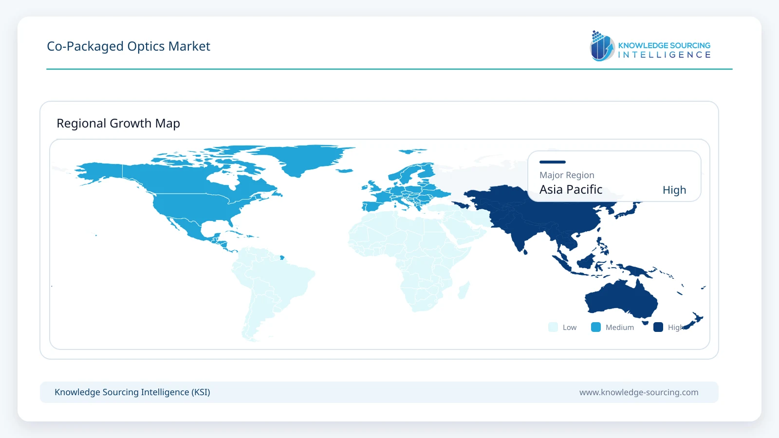
North America maintains strong commercial momentum due to extensive investment in hyperscale cloud infrastructure, AI computing platforms, semiconductor research, and advanced networking technologies. Major cloud service providers continue expanding domestic data center capacity while semiconductor companies accelerate development of next-generation switch architectures. Government initiatives supporting semiconductor manufacturing further strengthen regional supply capabilities.
Europe demonstrates steady demand supported by digital infrastructure modernization, sovereign cloud initiatives, and research computing investments. Telecommunications operators, research institutions, and industrial cloud providers are evaluating higher-capacity networking technologies to support data-intensive applications. Semiconductor packaging investments across several European countries also contribute to technology development, although manufacturing scale remains smaller than North America and parts of Asia.
Asia Pacific represents a major manufacturing and consumption region owing to extensive semiconductor production, optical component manufacturing, and rapidly expanding cloud infrastructure. China, Japan, South Korea, Taiwan, and India continue investing in advanced computing capacity, telecommunications modernization, and semiconductor supply chains. Regional manufacturers also play an important role in fiber optics, packaging equipment, and precision assembly technologies, strengthening the broader ecosystem.
The Middle East and Africa market is developing gradually as governments expand digital infrastructure, cloud services, and smart city initiatives. Demand is primarily concentrated within large data center projects and telecommunications modernization programs. Adoption remains constrained by comparatively limited hyperscale infrastructure and dependence on imported advanced optical technologies.
South America presents selective opportunities driven by cloud adoption, enterprise digitalization, and expanding telecommunications networks. Investment remains concentrated in larger economies where international cloud providers continue expanding regional infrastructure. Budget constraints and comparatively smaller AI computing deployments moderate the pace of widespread commercial adoption.
Competitive Landscape
The competitive structure combines global semiconductor companies, optical component manufacturers, silicon photonics innovators, automated packaging specialists, and fiber connectivity suppliers. Competition is determined by technological integration capability, manufacturing quality, packaging expertise, optical performance, and the ability to support future switch bandwidth generations.
Companies increasingly pursue strategic partnerships spanning semiconductor design, silicon photonics development, automated assembly, advanced testing, and fiber connectivity to reduce commercialization risk and accelerate product qualification. Collaboration between networking equipment suppliers and optical technology developers has become particularly important because successful deployment requires close integration across multiple hardware platforms.
Product differentiation focuses on power efficiency, optical engine density, thermal management, manufacturing scalability, and interoperability with evolving Ethernet standards. Geographic expansion strategies emphasize proximity to semiconductor manufacturing centers, advanced packaging facilities, and hyperscale cloud customers. The competitive environment includes Broadcom Inc., Lumentum Operations LLC, Ranovus, Ayar Labs, Inc., Cisco Systems, Inc., IBM Corporation, Corning Incorporated, ficonTEC Service GmbH, Furukawa Electric Co., Ltd., Hengtong Group Co., Ltd., and Hisense Broadband, Inc.
Recent Developments
July 2026: NVIDIA began shipping Spectrum-X CPO switches to select partners while Broadcom continued limited shipments of its 51.2T Bailly CPO switch, marking the transition of co-packaged optics into early volume production for AI infrastructure.
March 2026: At OFC 2026, Broadcom showcased its end-to-end AI optical networking portfolio, highlighting Taurus™ 400G/lane optical DSP, next-generation silicon photonics, and continued advancements toward volume-ready co-packaged optics for AI clusters.
March 2026: Founding members AMD, Broadcom, Meta, Microsoft, NVIDIA, and OpenAI established the Optical Scale-up Consortium (OCI MSA) to develop open specifications for optical interconnects, strengthening the multi-vendor ecosystem supporting future co-packaged optics deployments.
Regulatory and Policy Environment
The market operates within a framework of international networking standards, semiconductor manufacturing policies, environmental regulations, and telecommunications compliance requirements. Organizations including the IEEE, Optical Internetworking Forum (OIF), and Consortium for On-Board Optics (COBO) contribute technical specifications that improve interoperability and facilitate ecosystem development.
Government semiconductor initiatives, including domestic manufacturing incentive programs across North America, Europe, and Asia, are encouraging investment in advanced packaging, photonics research, and supply chain resilience. Environmental policies promoting energy-efficient digital infrastructure indirectly support adoption by encouraging lower-power networking technologies. Manufacturers must also comply with regulations governing hazardous substances, product safety, export controls, and environmental reporting throughout global supply chains.
Outlook and Strategic Implications
Commercial investment is expected to concentrate on scalable manufacturing, silicon photonics integration, automated packaging, thermal optimization, and high-density switching platforms capable of supporting future AI workloads. Procurement strategies among hyperscale operators will increasingly emphasize long-term operational efficiency, lifecycle economics, and supply chain resilience rather than initial hardware costs alone.
Technology development is likely to progress toward higher data rates, improved optical integration, and greater manufacturing automation, supporting broader commercialization across advanced networking environments. Strategic partnerships spanning semiconductor companies, photonics developers, packaging specialists, and networking vendors will remain central to reducing deployment complexity and accelerating qualification.
The principal commercial risks include manufacturing scalability, evolving interoperability standards, supply chain concentration, and the pace of customer migration from mature pluggable optical technologies. Nevertheless, organizations capable of delivering reliable production, validated energy savings, and seamless integration with next-generation switching architectures are expected to strengthen their competitive position as AI infrastructure investment continues to reshape global data center networking.
Co-Packaged Optics Market Scope
| Report Metric | Details |
|---|---|
| Forecast Unit | Billion |
| Study Period | 2021 to 2031 |
| Historical Data | 2021 to 2024 |
| Base Year | 2025 |
| Forecast Period | 2026 – 2031 |
| Segmentation | Data Rates, Application, Geography |
| Companies |
|
Market Segmentation
By Data Rate
By Application
By Geography
Table of Contents
1. EXECUTIVE SUMMARY
2. MARKET SNAPSHOT
2.1. Market Overview
2.2. Market Definition
2.3. Scope of the Study
2.4. Market Segmentation
3. BUSINESS LANDSCAPE
3.1. Market Drivers
3.2. Market Restraints
3.3. Market Opportunities
3.4. Porter’s Five Forces Analysis
3.5. Industry Value Chain Analysis
3.6. Policies and Regulations
3.7. Strategic Recommendations
4. TECHNOLOGICAL OUTLOOK
5. CO-PACKAGED OPTICS MARKET BY DATA RATE
5.1. Introduction
5.2. Less than 1.6T
5.3. 1.6T
5.4. 3.2T
5.5. 6.4T
6. CO-PACKAGED OPTICS MARKET BY APPLICATION
6.1. Introduction
6.2. Data Centers and High-Performance Computing (HPC)
6.3. Telecommunications and Networking
6.4. Others
7. CO-PACKAGED OPTICS MARKET BY GEOGRAPHY
7.1. Introduction
7.2. North America
7.2.1. By Data Rate
7.2.2. By Application
7.2.3. By Country
7.2.3.1. USA
7.2.3.2. Canada
7.2.3.3. Mexico
7.3. South America
7.3.1. By Data Rate
7.3.2. By Application
7.3.3. By Country
7.3.3.1. Brazil
7.3.3.2. Argentina
7.3.3.3. Others
7.4. Europe
7.4.1. By Data Rate
7.4.2. By Application
7.4.3. By Country
7.4.3.1. United Kingdom
7.4.3.2. Germany
7.4.3.3. France
7.4.3.4. Spain
7.4.3.5. Others
7.5. Middle East and Africa
7.5.1. By Data Rate
7.5.2. By Application
7.5.3. By Country
7.5.3.1. Saudi Arabia
7.5.3.2. UAE
7.5.3.3. Others
7.6. Asia Pacific
7.6.1. By Data Rate
7.6.2. By Application
7.6.3. By Country
7.6.3.1. China
7.6.3.2. Japan
7.6.3.3. India
7.6.3.4. South Korea
7.6.3.5. Taiwan
7.6.3.6. Others
8. COMPETITIVE ENVIRONMENT AND ANALYSIS
8.1. Major Players and Strategy Analysis
8.2. Market Share Analysis
8.3. Mergers, Acquisitions, Agreements, and Collaborations
8.4. Competitive Dashboard
9. COMPANY PROFILES
9.1. Broadcom Inc.
9.2. Lumentum Operations LLC
9.3. Ranovus
9.4. Ayar Labs, Inc.
9.5. Cisco Systems, Inc.
9.6. IBM Corporation
9.7. Corning Incorporated
9.8. ficonTEC Service GmbH
9.9. Furukawa Electric Co., Ltd.
9.10. Hengtong Group Co., Ltd.
9.11. Hisense Broadband, Inc.
10. APPENDIX
10.1. Currency
10.2. Assumptions
10.3. Base and Forecast Years Timeline
10.4. Key Benefits for Stakeholders
10.5. Research Methodology
10.6. Abbreviations
Navigate
Trusted by the world's leading organizations











