
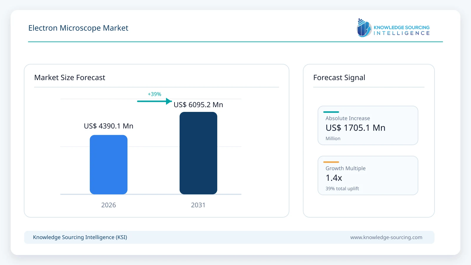
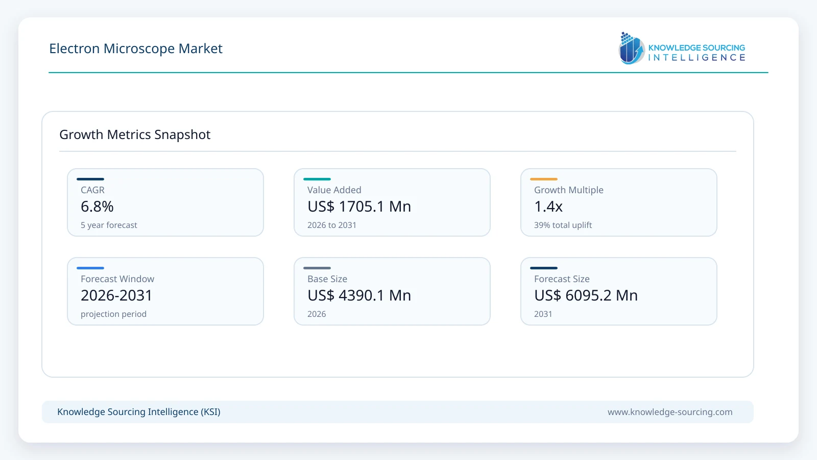
The electron microscope market is set to reach USD 6,095.22 million in 2031, growing at a CAGR of 6.78% from a valuation of USD 4,390.08 million in 2026.
Highlights:
- 1Demand increasingly reflects strategic investment in semiconductor fabrication, structural biology, and advanced materials characterization.
- 2Cryogenic electron microscopy continues to expand pharmaceutical and biotechnology research applications through high-resolution molecular imaging.
- 3Semiconductor process miniaturization is increasing demand for high-resolution failure analysis and nanoscale metrology tools.
- 4Instrument manufacturers are investing in automation, AI-enabled workflows, and expanded service capabilities to improve laboratory productivity.
- 5High capital expenditure, infrastructure requirements, and skilled workforce shortages remain important constraints across end-user industries.
Unlike optical microscopy, electron microscopy enables imaging and characterization at nanometer and sub-nanometer scales, allowing researchers and manufacturers to investigate material composition, structural defects, biological specimens, and semiconductor devices with substantially higher resolution. Demand increasingly reflects the need for precise structural information rather than routine visualization, making purchasing decisions highly dependent on analytical performance, automation capability, software integration, service availability, and long-term operating costs.
Investment patterns have broadened beyond academic laboratories. Semiconductor manufacturers continue expanding process-control capabilities for advanced nodes, while pharmaceutical companies increasingly incorporate cryogenic electron microscopy (Cryo-EM) into biologics discovery and structure-based drug development. Materials science laboratories, battery developers, and government research organizations are also increasing investment in high-resolution imaging platforms to accelerate product development and improve analytical accuracy. The continued expansion of Cryo-EM infrastructure supported by national research programs further improves instrument accessibility and workforce development.
Competition is concentrated among a limited number of global manufacturers with extensive expertise in electron optics, vacuum engineering, detectors, automation software, and lifecycle services. Purchasing decisions increasingly extend beyond instrument specifications to include application support, workflow automation, image-processing software, service contracts, operator training, and compatibility with laboratory information systems. As analytical workflows become more data intensive, suppliers are integrating artificial intelligence, automated image acquisition, and cloud-enabled data management to improve throughput and reduce operator dependence. Recent product introductions also indicate efforts to broaden adoption by reducing laboratory infrastructure requirements while maintaining high imaging performance.
Key Market Indicators
Indicator | Latest Evidence | Commercial Meaning |
NIH Cryo-EM Service Centers | National centers transitioned to sustained NIGMS support (2024) | Long-term public investment strengthens life-science research infrastructure. |
National CryoET Network | Supported through August 2026 | Continued funding expands access to advanced biological imaging capabilities. |
Thermo Fisher Product Launch | Glacios 3 Cryo-TEM introduced in 2026 | Suppliers are lowering infrastructure barriers for broader laboratory adoption. |
Customer Base | Pharmaceutical, biotechnology, academic, government, industrial and semiconductor customers | Demand is diversified across research and commercial end users. |
Technology Direction | Increasing AI integration with scientific instrumentation | Automation is becoming an important competitive differentiator. |
Key indicator: NIH-supported Cryo-EM service centers continue under sustained National Institute of General Medical Sciences funding.
Commercial meaning: Stable public infrastructure lowers access barriers for advanced structural biology while supporting long-term instrument utilization.
Market Drivers
Semiconductor process complexity is increasing analytical requirements. Shrinking transistor geometries, advanced packaging technologies, and heterogeneous chip integration require higher-resolution defect inspection, failure analysis, and process validation. Semiconductor manufacturers increasingly depend on scanning electron microscopes, transmission electron microscopes, and focused ion beam systems throughout process development and yield improvement. Suppliers continue expanding automation, detector performance, and analytical software because customers require faster inspection cycles without compromising measurement precision. These requirements are expected to remain commercially important as advanced-node manufacturing expands across North America, Europe, and Asia Pacific.
Structural biology and biologics development continue expanding Cryo-EM adoption. Pharmaceutical and biotechnology organizations increasingly use Cryo-EM to determine protein structures that are difficult to characterize using conventional crystallography. NIH-supported Cryo-EM programs, national service centers, and workforce training initiatives have expanded researcher access while improving technical capability across academic and translational research institutions. Instrument manufacturers are responding by introducing systems that reduce installation constraints and simplify operation, enabling broader deployment beyond specialized national laboratories. These developments strengthen recurring demand for both instruments and associated analytical services.
Advanced materials, battery research, and nanotechnology require higher-resolution characterization. Battery developers, advanced materials producers, aerospace manufacturers, and nanotechnology researchers increasingly rely on electron microscopy to examine crystal structures, interfaces, degradation mechanisms, and manufacturing defects. Public and private investment in next-generation batteries, lightweight materials, and functional nanomaterials continues expanding analytical workloads. Manufacturers are therefore investing in higher detector sensitivity, automated workflows, and in-situ microscopy capabilities that enable observation of structural changes during material testing, providing customers with more comprehensive analytical information than conventional static imaging.
Automation and AI-enabled workflows are improving laboratory productivity. Modern electron microscopy increasingly depends on software-assisted image acquisition, automated alignment, data management, and artificial intelligence to reduce operator workload while improving reproducibility. Thermo Fisher Scientific recently announced collaborations combining laboratory instrumentation with AI capabilities alongside new Cryo-TEM platforms designed for broader laboratory deployment. These investments reflect customer demand for shorter analysis times, standardized workflows, and improved utilization of high-value instruments, particularly where skilled microscopy specialists remain limited.
Market Restraints and Challenges
High ownership costs extend procurement cycles. Electron microscopes require substantial investment beyond instrument acquisition. Facilities often need vibration isolation, controlled environmental conditions, vacuum infrastructure, stable electrical supply, specialized cooling systems, and long-term service agreements. Academic institutions and smaller industrial laboratories frequently depend on government grants or centralized facilities before purchasing high-end systems, extending procurement timelines and limiting broader commercial adoption. Suppliers increasingly respond by developing instruments with reduced infrastructure requirements, but capital intensity remains an important market constraint.
Shortage of experienced microscopy specialists limits instrument utilization. Advanced transmission electron microscopy, Cryo-EM, and FIB-SEM systems require specialized expertise in sample preparation, instrument calibration, image processing, and data interpretation. NIH has acknowledged that broader Cryo-EM adoption has historically been constrained by limited equipment access and workforce availability, prompting national investments in training and service centers. Although these initiatives improve long-term capacity, workforce development remains slower than expanding research demand across pharmaceutical, biotechnology, and materials science applications.
Complex sample preparation affects productivity and operating cost. High-resolution imaging frequently requires demanding preparation techniques, particularly for biological specimens, semiconductor cross-sections, and nanomaterials. Sample preparation introduces additional equipment requirements, operator time, and opportunities for analytical variability. Laboratories therefore evaluate complete workflow efficiency rather than microscope performance alone when selecting suppliers. Manufacturers continue investing in integrated sample preparation solutions, workflow software, and automation to reduce preparation errors, but sample complexity remains an operational challenge across several end-user industries.
Rapid technological evolution increases replacement pressure and investment risk. Continuous improvements in detectors, automation software, image reconstruction algorithms, and in-situ analytical capabilities shorten technology cycles for premium instruments. Research organizations and industrial laboratories must balance the benefits of adopting newer platforms against budget constraints and long equipment depreciation periods. Manufacturers address this challenge through modular upgrades, software enhancements, and lifecycle service programs, yet technology refresh decisions continue to influence procurement timing and capital allocation across the market.
Major Segment Analysis
Semiconductor and Electronics
Semiconductor and electronics applications represent one of the most commercially important demand segments for electron microscopes because device scaling, advanced packaging, and heterogeneous integration require imaging and analytical capabilities beyond the limits of optical inspection. Scanning electron microscopes (SEM), transmission electron microscopes (TEM), and focused ion beam-scanning electron microscopes (FIB-SEM) support wafer inspection, defect localization, process validation, failure analysis, and nanoscale metrology throughout research, pilot production, and volume manufacturing. As integrated circuit architectures become increasingly complex, manufacturers require higher imaging resolution, elemental analysis, and automated inspection workflows to maintain yield and shorten development cycles.
Purchasing decisions in this segment emphasize throughput, analytical precision, software integration, and service responsiveness rather than instrument resolution alone. Semiconductor manufacturers also require compatibility with automated sample handling, process data management, and artificial intelligence-assisted defect classification to improve productivity. Suppliers therefore compete through detector performance, automation capabilities, application expertise, and global service infrastructure, while long qualification cycles and demanding customer specifications continue to create high entry barriers for new competitors.
Regional Analysis
Region | Main Demand Signal | Principal Constraint |
North America | Semiconductor investment, pharmaceutical research, federally supported scientific infrastructure | High acquisition and operating costs |
Europe | Advanced manufacturing, life sciences research, collaborative research funding | Lengthy public procurement and budget constraints |
Asia Pacific | Semiconductor fabrication, electronics manufacturing, government R&D investment | Supply-chain dependence for selected high-end components |
Middle East and Africa | Expansion of national research capability and healthcare infrastructure | Limited installed research base and specialist workforce |
The United States remains one of the largest centers for electron microscope deployment because of sustained investment in semiconductor manufacturing, biomedical research, nanotechnology, and national laboratory infrastructure. Federal initiatives supporting semiconductor manufacturing, together with NIH-funded Cryo-EM service centers and structural biology programs, continue expanding demand across both academic and industrial laboratories. Canada complements regional demand through publicly funded research institutions, while Mexico increasingly supports industrial inspection associated with electronics manufacturing and automotive supply chains.
European demand is supported by advanced manufacturing, materials science, pharmaceutical research, and collaborative scientific programs. Germany, the United Kingdom, France, and the Netherlands maintain extensive research infrastructure and host several internationally recognized microscopy facilities. Regional demand also benefits from aerospace engineering, automotive innovation, and battery research. Procurement cycles, however, are often influenced by public funding availability and institutional budgeting, extending purchasing timelines for high-value analytical instruments.
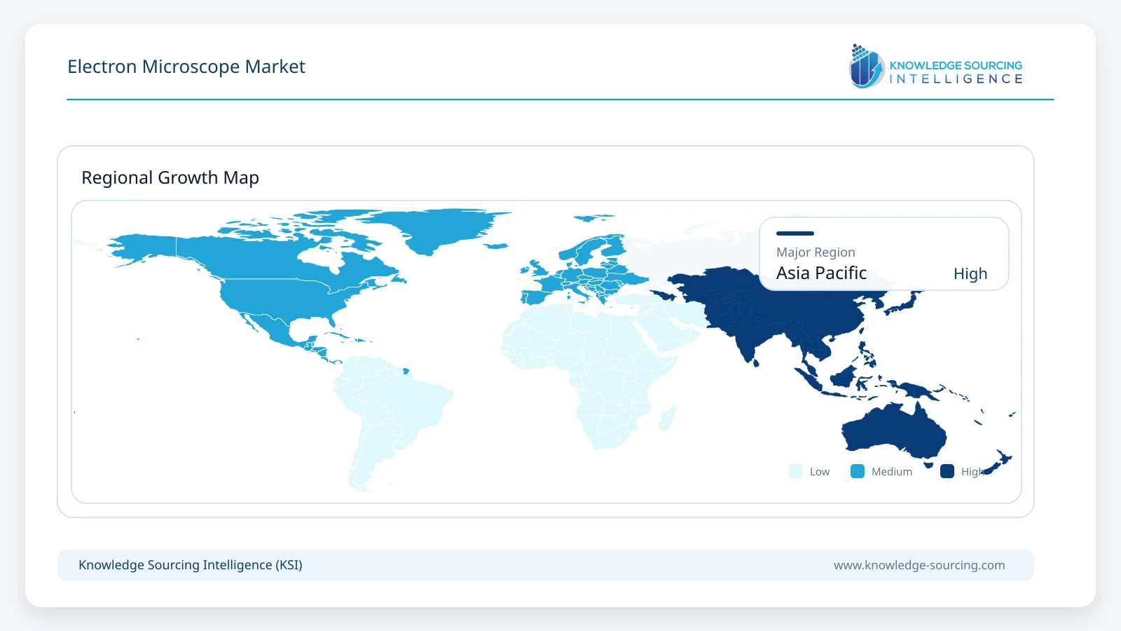
Asia Pacific continues to represent one of the most active investment regions because of its concentration of semiconductor fabrication, electronics manufacturing, precision engineering, and government-supported research initiatives. China, Japan, South Korea, and Taiwan continue investing in semiconductor production capacity and advanced materials research, while India is expanding scientific infrastructure through increased public research funding. These investments support demand for electron microscopy across quality control, process development, and research applications. The presence of regional manufacturers also strengthens local service capability and application support.
Middle East and Africa remain comparatively smaller markets but continue expanding research capabilities through investments in healthcare, university research, and national innovation programs. Countries including Saudi Arabia and the United Arab Emirates have increased investment in scientific infrastructure as part of broader economic diversification strategies. Although installation volumes remain lower than in North America, Europe, or Asia Pacific, gradual expansion of research capacity is creating additional opportunities for suppliers offering training, application support, and long-term service agreements.
Competitive Landscape
Competition remains concentrated among a relatively small group of manufacturers possessing expertise in electron optics, precision engineering, detector technology, vacuum systems, and analytical software. Thermo Fisher Scientific, JEOL Ltd., Hitachi High-Tech Corporation, Carl Zeiss AG, TESCAN ORSAY HOLDING, Bruker Corporation, Oxford Instruments plc, Delong Instruments, COXEM, Nion, SEC Co., Ltd., and Delmic BV compete across research, industrial, semiconductor, and life science applications through differentiated product portfolios and specialized application support.
Competitive positioning increasingly depends on complete workflow capability rather than instrument specifications alone. Manufacturers continue investing in automation, artificial intelligence-assisted imaging, improved detectors, integrated sample preparation, and digital workflow software to improve laboratory productivity. Expansion of global service networks, operator training, lifecycle maintenance, and application consulting has also become an important competitive factor because customers increasingly evaluate total cost of ownership and long-term operational reliability. High research and development requirements, extensive customer qualification processes, established service infrastructure, and technological complexity continue to create substantial barriers for new market entrants.
Recent Developments
March 2026: Thermo Fisher Scientific launched the Glacios 3 Cryo-Transmission Electron Microscope. The system integrates advanced automation and high-throughput capabilities, drastically streamlining high-resolution structural biology and cryo-EM drug discovery workflows.
December 2025: Hitachi High-Tech announced the HT7800II Transmission Electron Microscope. Designed for high operational efficiency, it features advanced digital technologies for high-quality data acquisition across biomaterial and nanotechnology research applications.
October 2025: Hitachi High-Tech launched the SU9600, a next-generation ultrahigh-resolution scanning electron microscope. Equipped with a stable cold field-emission source, it delivers 0.4 nm resolution alongside enhanced automated throughput.
2025: Thermo Fisher Scientific launched the Vulcan Automated Lab, leveraging AI and robotics to transform atomic-scale semiconductor analysis with automated TEM metrology.
2025: Thermo Fisher released the Krios 5 Cryo-TEM, incorporating AI-driven automation to accelerate molecular structure studies in biological research.
Regulatory and Policy Environment
Government research funding, laboratory accreditation requirements, and semiconductor industrial policies continue shaping demand across the electron microscope market. In the United States, the National Institutes of Health (NIH) and the National Institute of General Medical Sciences (NIGMS) continue supporting Cryo-EM service centers and workforce development programs, improving national access to high-resolution structural biology infrastructure. Similar investments across Europe and Asia support collaborative scientific research, advanced manufacturing, and nanotechnology development.
Electron microscope manufacturers must also comply with international product safety standards, export control regulations, environmental requirements, and quality management systems governing scientific instrumentation. Sales involving advanced analytical equipment may require export licensing depending on destination country and product capability. Regulatory compliance therefore affects product development, international distribution strategies, customer qualification processes, and after-sales support. Manufacturers increasingly incorporate cybersecurity, digital data management, and software lifecycle support into product development as laboratories adopt more connected analytical workflows.
Outlook and Strategic Implications
Demand during the 2026–2031 forecast period is expected to remain closely linked to semiconductor technology development, structural biology research, advanced materials engineering, battery innovation, and nanotechnology commercialization rather than broad laboratory expansion alone. Continued investment in artificial intelligence-assisted microscopy, workflow automation, and integrated analytical software is expected to improve instrument utilization while reducing dependence on highly specialized operators.
Several strategic priorities are expected to influence market performance:
Manufacturers: Expand automation, application-specific solutions, and lifecycle service offerings while strengthening regional support capabilities.
Research institutions: Increase shared laboratory infrastructure and workforce training to improve utilization of high-value analytical systems.
Semiconductor and industrial users: Prioritize instruments offering higher throughput, workflow integration, and lower total ownership costs.
Pharmaceutical and biotechnology organizations: Continue expanding Cryo-EM capacity for biologics discovery and structure-based drug development where molecular characterization directly supports research productivity.
Long-term competition is expected to remain technology driven, with differentiation increasingly determined by software capability, automation, analytical workflows, service quality, and application expertise rather than imaging resolution alone. Suppliers capable of combining high-performance instrumentation with comprehensive lifecycle support and digital laboratory integration are expected to strengthen their competitive position as customer purchasing decisions increasingly emphasize operational efficiency and long-term productivity.
Electron Microscope Market Scope:
| Report Metric | Details |
|---|---|
| Total Market Size in 2026 | USD 4,390.08 million |
| Total Market Size in 2031 | USD 6,095.22 million |
| Forecast Unit | Million |
| Growth Rate | 6.78% |
| Study Period | 2021 to 2031 |
| Historical Data | 2021 to 2024 |
| Base Year | 2025 |
| Forecast Period | 2026 – 2031 |
| Segmentation | Product Type , Technology , Application, End User, Geography |
| Companies |
|
Market Segmentation
By Product Type
By Technology
By Application
By End User
By Geography
Table of Contents
1. EXECUTIVE SUMMARY
2. MARKET SNAPSHOT
2.1. Market Overview
2.2. Market Definition
2.3. Scope of the Study
2.4. Market Segmentation
3. BUSINESS LANDSCAPE
3.1. Market Drivers
3.2. Market Restraints
3.3. Market Opportunities
3.4. Porter’s Five Forces Analysis
3.5. Industry Value Chain Analysis
3.6. Policies and Regulations
3.7. Strategic Recommendations
4. TECHNOLOGICAL OUTLOOK
5. ELECTRON MICROSCOPE MARKET BY PRODUCT TYPE
5.1. Introduction
5.2. Scanning Electron Microscope
5.3. Transmission Electron Microscope
5.4. Scanning Transmission Electron Microscope (STEM)
5.5. Focused Ion Beam-Scanning Electron Microscope (FIB-SEM)
6. ELECTRON MICROSCOPE MARKET BY TECHNOLOGY
6.1. Introduction
6.2. Conventional High-Vacuum Electron Microscopy
6.3. Cryogenic Electron Microscopy (Cryo-EM)
6.4. Environmental / Variable Pressure EM (ESEM)
6.5. Low-Voltage Electron Microscopy
6.6. In-situ Electron Microscopy
7. ELECTRON MICROSCOPE MARKET BY APPLICATION
7.1. Introduction
7.2. Material Sciences
7.3. Life Sciences and Biotechnology
7.4. Nanotechnology
7.5. Semiconductor and Electronics
7.6. Pharmaceuticals
7.7. Forensic Science
7.8. Geology and Earth Sciences
7.9. Energy and Battery Research
8. ELECTRON MICROSCOPE MARKET BY END USER
8.1. Introduction
8.2. Academic and Research Institutions
8.3. Semiconductor and Electronics Manufacturers
8.4. Industrial Manufacturing
8.5. Government and National Laboratories
8.6. Pharmaceutical and Biotechnology Companies
8.7. Contract Research Organizations (CROs)
9. ELECTRON MICROSCOPE MARKET BY GEOGRAPHY
9.1. Introduction
9.2. North America
9.2.1. United States
9.2.2. Canada
9.2.3. Mexico
9.3. South America
9.3.1. Brazil
9.3.2. Argentina
9.3.3. Others
9.4. Europe
9.4.1. United Kingdom
9.4.2. Germany
9.4.3. France
9.4.4. Spain
9.4.5. Others
9.5. Middle East and Africa
9.5.1. Saudi Arabia
9.5.2. UAE
9.5.3. Others
9.6. Asia Pacific
9.6.1. China
9.6.2. India
9.6.3. Japan
9.6.4. South Korea
9.6.5. Indonesia
9.6.6. Thailand
9.6.7. Others
10. COMPETITIVE ENVIRONMENT AND ANALYSIS
10.1. Major Players and Strategy Analysis
10.2. Market Share Analysis
10.3. Mergers, Acquisitions, Agreements, and Collaborations
10.4. Competitive Dashboard
11. COMPANY PROFILES
11.1. Thermo Fisher Scientific
11.2. JEOL Ltd.
11.3. Hitachi High-Tech Corporation
11.4. Carl Zeiss AG
11.5. TESCAN ORSAY HOLDING, a.s.
11.6. Bruker Corporation
11.7. Oxford Instruments plc
11.8. Delong Instruments Inc.
11.9. COXEM Co., Ltd.
11.10. Nion Company
11.11. SEC Co., Ltd. (Korea)
11.12. Delmic BV
12. RESEARCH METHODOLOGY
Navigate
Trusted by the world's leading organizations











