
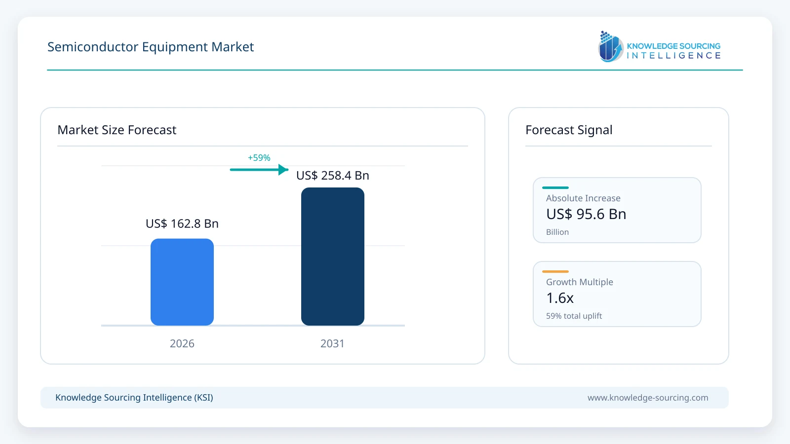
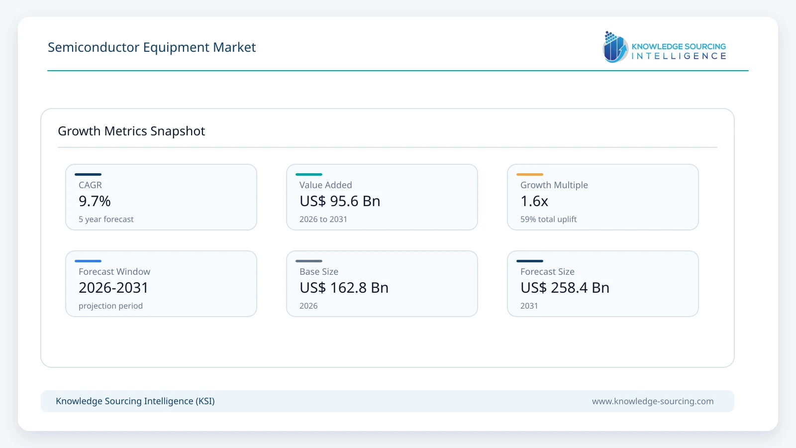
The Semiconductor Equipment Market is projected to expand at a CAGR of 9.7%, reaching USD 258.4 billion in 2031 from USD 162.8 billion in 2026.
Highlights:
- 1Front-end equipment accounts for approximately 87% of global semiconductor equipment market value in 2026, reflecting the high capital intensity of wafer fabrication.
- 2Foundries account for approximately 44% of equipment demand in 2026, supported by leading-edge logic and advanced-node capacity investment.
- 32D semiconductor architectures account for approximately 57% of market value in 2026, although 2.5D and 3D equipment requirements are increasing faster.
- 4Asia Pacific accounts for approximately 83% of global semiconductor equipment demand in 2026, reflecting the concentration of semiconductor fabrication and packaging capacity.
- 5China accounts for approximately 31% of market value in 2026, remaining the largest individual equipment market while domestic suppliers increase their participation.
Semiconductor equipment includes systems used in front-end wafer fabrication and back-end assembly, packaging and testing. Front-end equipment covers lithography, deposition, etching, cleaning, ion implantation, chemical mechanical planarization, wafer inspection, metrology and related manufacturing processes. Back-end equipment includes wafer probing, dicing, bonding, assembly, packaging, inspection and semiconductor test systems.
The industry's revenue base is supported by a concentrated group of large suppliers operating across highly specialized process categories. ASML remains central to advanced lithography, while Applied Materials, Lam Research and Tokyo Electron compete across multiple wafer-processing technologies. KLA maintains a strong position in process control, Advantest and Teradyne participate prominently in semiconductor test, and companies such as ASMPT, Besi and DISCO address important back-end and packaging processes.
The competitive landscape is also becoming more geographically diverse. Chinese suppliers such as NAURA Technology, AMEC, Piotech and ACM Research have expanded rapidly across deposition, etch, cleaning and related equipment categories, while established Japanese, European and US manufacturers continue investing heavily in next-generation process technology.
Growth through 2031 is expected to remain uneven rather than follow a uniform annual trajectory. Strong AI-related investment is supporting rapid expansion during the early part of the forecast period, although semiconductor capital expenditure remains cyclical and periods of digestion are expected as manufacturers absorb previously installed capacity.
Market Trends
AI Is Increasing Manufacturing Complexity Across Logic, Memory and Packaging
Artificial intelligence is creating a broader semiconductor equipment cycle than demand generated by a single device category. AI accelerators require advanced logic, large quantities of HBM and increasingly sophisticated packaging architectures, meaning spending is occurring across several manufacturing stages simultaneously.
Leading-edge processors require more advanced patterning, deposition, etching and inspection, while HBM increases the need for advanced DRAM processing, die stacking and testing. Packaging also becomes more important because compute performance increasingly depends on connecting multiple logic and memory dies efficiently rather than relying solely on monolithic scaling.
This combination strengthens demand across a larger group of equipment suppliers. Front-end companies benefit from additional process complexity, while test, bonding and inspection providers gain from the increasing number of dies and interfaces within high-performance semiconductor packages.
High-NA EUV Is Moving Closer to Broader Production Adoption
EUV lithography has become central to advanced logic production, and the next transition is toward High Numerical Aperture EUV. The technology provides higher patterning resolution and is intended to support future nodes while reducing some of the multiple-patterning complexity associated with continued scaling.
Intel Foundry and ASML reported further High-NA progress in September 2026, with the technology already being used on selected production layers. ASML and TSMC are also working on a larger photomask format intended to improve future High-NA system productivity.
Its impact extends beyond lithography itself because new patterning approaches influence resist processing, etching, deposition and metrology requirements. High-NA adoption therefore supports a wider ecosystem of process-equipment investment as manufacturers prepare for sub-2nm and subsequent logic generations.
HBM Is Reshaping Memory Equipment Spending
High-bandwidth memory has become one of the strongest investment areas within semiconductor manufacturing because AI processors require extremely high memory bandwidth and close physical integration between compute and memory.
HBM demand supports conventional DRAM wafer fabrication but adds further manufacturing requirements during stacking, bonding, inspection and test. Advantest, for example, has reported exceptionally strong demand for semiconductor test systems linked to AI and high-performance memory, while equipment suppliers across deposition and process control are benefiting from more advanced DRAM manufacturing requirements.
The result is a memory cycle in which value growth can exceed wafer growth. Each HBM device incorporates more complex processing and back-end steps than conventional memory, increasing equipment content across the manufacturing flow.
Advanced Packaging Is Blurring the Front-End and Back-End Boundary
Chiplet architectures, 2.5D integration, 3D stacking and hybrid bonding are changing the traditional distinction between wafer fabrication and semiconductor packaging. Processes once concentrated primarily inside the wafer fab are increasingly required at advanced packaging stages, particularly when very fine-pitch interconnects and wafer-level bonding are involved.
Applied Materials, Tokyo Electron, Besi, ASMPT, Onto Innovation and other suppliers are expanding products targeting heterogeneous integration and advanced bonding. Test requirements are also increasing because manufacturers need to identify defective dies before combining multiple expensive components into a single package.
This shift raises the strategic importance of back-end equipment and creates opportunities for companies that can transfer precision manufacturing technologies from wafer processing into packaging.
Market Drivers
Advanced Logic Manufacturing Requires Greater Equipment Intensity
The transition toward 2nm and subsequent semiconductor nodes involves new transistor structures, more demanding patterning and increasingly complex materials engineering. Gate-all-around architectures require extremely precise deposition and etch processes, while advanced interconnect structures add further process steps.
These changes mean equipment spending can increase even when wafer capacity expands more moderately. Applied Materials introduced new deposition and selective etch systems in June 2026 to address increasingly complex 3D logic and memory structures, while Lam Research is working with IBM on process technologies intended for logic scaling beyond 1nm.
Such technology transitions provide a recurring source of equipment demand because leading semiconductor manufacturers must upgrade process capability as each node moves into volume production.
Memory Technology Transitions Are Supporting Another Capital Investment Cycle
HBM, advanced DRAM and higher-layer NAND are increasing capital requirements across memory manufacturing. DRAM suppliers need additional capacity and more advanced process technology to serve AI infrastructure, while NAND manufacturers continue increasing layer counts to raise storage density.
Higher-layer structures require increasingly demanding deposition and etch processes, while smaller DRAM features increase lithography, process-control and materials requirements. These shifts improve equipment intensity per wafer even when underlying unit demand grows more slowly.
The resulting cycle supports both specialized memory-equipment suppliers and diversified companies serving logic and memory customers.
Semiconductor Localization Is Broadening Global Equipment Investment
The semiconductor industry remains concentrated in Asia, but government incentives and supply-chain resilience initiatives are supporting new fabs and packaging facilities in the United States, Japan, Europe and India.
New greenfield facilities require broad equipment sets rather than isolated replacement tools, creating demand across lithography, deposition, etching, cleaning, inspection, metrology and test. Suppliers also benefit from service infrastructure, process development and future capacity additions around these sites.
Regional diversification does not remove Asia Pacific's dominance during the forecast period, but it gradually creates a broader equipment demand base and increases the strategic importance of local manufacturing and support capabilities.
Market Restraints and Challenges
Semiconductor Capital Expenditure Remains Cyclical
Equipment demand can change quickly when semiconductor manufacturers alter capacity plans. Strong investment periods may be followed by slower spending as foundries, memory producers and IDMs absorb previously installed capacity and respond to inventory conditions.
The current AI-driven cycle has generated strong demand, particularly in advanced logic and memory, but it does not eliminate the industry's historical investment volatility. Equipment manufacturers therefore need to manage manufacturing capacity, inventories and supplier commitments against rapidly changing customer schedules.
Companies with diversified exposure across process categories and semiconductor applications are better positioned to manage these fluctuations than suppliers dependent on a single technology or customer group.
Export Controls Are Reshaping Supplier Access and Competition
Advanced semiconductor equipment is increasingly subject to export restrictions because governments view leading-edge chipmaking technology as strategically important. These controls can restrict sales of selected systems into China and create uncertainty around licensing, product configurations and customer investment plans.
At the same time, restrictions are accelerating localization within China. NAURA Technology, AMEC, Piotech and other domestic equipment suppliers have increased revenue and market participation as Chinese semiconductor manufacturers seek locally available alternatives.
International suppliers continue to participate extensively in the Chinese market, particularly in permitted process technologies, but their competitive environment is changing as domestic vendors expand into a wider range of production steps.
Segment Analysis
By Equipment Type: Front-End Equipment
Front-end equipment is projected to generate approximately USD 218 billion by 2031, remaining the largest equipment category. It includes the systems required to build semiconductor devices on wafers, covering lithography, deposition, etching, cleaning, implantation, planarization and process control.
Its value is supported by the increasing number and complexity of process steps required for advanced logic and memory. Gate-all-around transistors, HBM, higher-layer NAND and future device structures require finer dimensional control and more sophisticated materials engineering, increasing demand for specialized tools.
ASML, Applied Materials, Lam Research, Tokyo Electron and KLA account for a substantial proportion of the segment, while ASM, SCREEN, Hitachi High-Tech, Kokusai Electric and a growing group of Chinese suppliers compete in specific process categories. Back-end equipment grows faster through 2031 as advanced packaging and test become more technically demanding, but front-end systems continue to represent the majority of overall industry value.
By End-User: Foundries
Foundries are projected to generate approximately USD 116 billion in semiconductor equipment demand by 2031, remaining the largest end-user category. Their spending is driven by leading-edge logic capacity, process-node migration and continued expansion of mature and specialty manufacturing technologies.
TSMC, Samsung Foundry, GlobalFoundries, SMIC and other foundries invest across a wide range of equipment categories because each new fabrication line requires an integrated collection of lithography, etch, deposition, cleaning and process-control systems.
AI-related processors are strengthening demand for advanced-node foundry capacity, while automotive, industrial and connectivity applications continue supporting established nodes. IDMs remain another major buyer group, particularly in memory and advanced logic, while OSAT companies account for a smaller but increasingly important equipment pool as packaging complexity grows.
By Dimension: 2D
2D semiconductor manufacturing is projected to generate approximately USD 130 billion in equipment demand by 2031, retaining the largest share of the dimension-based market even as its relative position declines.
Conventional planar and primarily two-dimensional semiconductor structures remain widely used across mature logic, analog, power, automotive and industrial applications. Large installed manufacturing bases and continued expansion at established nodes create recurring equipment requirements across these applications.
However, future growth increasingly shifts toward 2.5D and 3D manufacturing. Chiplets, HBM stacks, hybrid bonding and vertically integrated device structures create additional opportunities for advanced bonding, deposition, inspection and metrology equipment, gradually increasing their share of industry investment.
Regional Analysis
Major Region: Asia Pacific
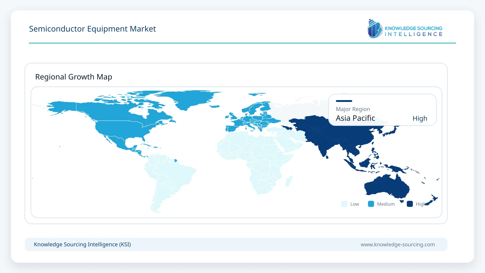
Asia Pacific is projected to generate approximately USD 207 billion in semiconductor equipment revenue by 2031, maintaining its dominant position throughout the forecast period.
Taiwan remains central to advanced foundry manufacturing, South Korea combines major memory and foundry investment, China maintains extensive production capacity across mature and selected advanced nodes, and Japan continues investing in logic, memory, power and specialty semiconductor manufacturing.
The region is also home to a large proportion of the equipment supply chain. Tokyo Electron, Advantest, SCREEN, Hitachi High-Tech, Kokusai Electric, DISCO, Nikon and Canon are headquartered in Japan, while Chinese suppliers are expanding rapidly across multiple process categories.
Manufacturing investments in North America and Europe gradually reduce Asia Pacific's share, but the scale of existing fabs, packaging operations and planned capacity additions ensures that it remains the principal semiconductor equipment market through 2031.
Major Country: China
China is projected to generate approximately USD 67 billion in semiconductor equipment revenue by 2031, remaining the largest individual national market despite a gradual reduction in its share of global spending.
Demand is supported by continued investment in domestic foundry, memory and specialty semiconductor capacity. Mature and established-node production remains particularly important, while companies are also investing in technologies where advanced equipment remains available.
The supplier structure is changing rapidly. NAURA has emerged as one of the world's largest semiconductor equipment manufacturers, while AMEC has expanded in etching and thin-film systems and companies such as Piotech, ACM Research, Kingsemi and Hwatsing are developing stronger positions in deposition, cleaning, CMP and other process categories.
This localization creates greater competition for international equipment vendors but also expands the overall depth of China's semiconductor manufacturing ecosystem.
Competitive Environment and Analysis
The semiconductor equipment market is characterized by high technological barriers, extensive customer qualification requirements and strong supplier positions within individual process categories. Competition occurs less through commodity pricing and more through process performance, yield improvement, throughput, reliability and the ability to support customers during technology transitions.
Applied Materials maintains one of the industry's broadest equipment portfolios across deposition, etch, implantation, CMP and other materials-engineering processes. Lam Research has particularly strong exposure to etch and deposition, while Tokyo Electron participates across coating and developing, etching, deposition, cleaning and wafer probing. KLA occupies a central position in inspection, metrology and process control.
ASML holds a unique position in advanced lithography and remains the only commercial supplier of EUV systems. Its technology roadmap therefore influences equipment investment across the broader manufacturing ecosystem because each lithography transition also creates requirements for adjacent patterning, inspection and process technologies.
Competition differs in the back-end market. Advantest and Teradyne are major semiconductor test suppliers, while ASMPT, Besi, DISCO and other specialists serve bonding, assembly, dicing and advanced packaging applications. The rapid development of HBM and chiplet-based architectures is increasing the strategic importance of these suppliers.
Chinese manufacturers are becoming more significant competitors. NAURA has expanded across several front-end categories, AMEC competes in etching and deposition, and Piotech has grown rapidly in thin-film equipment. Their development is particularly important within China, where customers are increasing local equipment procurement.
Recent Developments
September 2026: Intel Foundry and ASML reported further progress in High-NA EUV manufacturing, with the technology being used on selected production layers and more than one million wafers processed across development, qualification and production activities.
September 2026: Axcelis Technologies announced a USD 35 million investment in a new ion implantation equipment manufacturing facility in Pyeongtaek, South Korea.
July 2026: Tokyo Electron expanded its collaboration with NVIDIA around agentic AI, digital twins and robotics for semiconductor manufacturing operations and equipment maintenance.
June 2026: Advantest and OpenLight announced plans to develop high-volume silicon photonics test solutions for optical engines used in AI and high-performance data-center infrastructure.
June 2026: Applied Materials introduced the Centris Spectral SiN ALD and Producer Selectra Mo Etch systems for increasingly complex 3D logic and memory manufacturing.
March 2026: IBM and Lam Research entered a five-year collaboration focused on materials, etch, deposition and High-NA EUV processes for future sub-1nm logic technologies.
Market Outlook
The global semiconductor equipment market is forecast to increase. The expansion is supported by simultaneous investment across advanced logic, HBM, DRAM, NAND, semiconductor test and advanced packaging.
AI remains the strongest near-term catalyst, but the underlying driver is increasing manufacturing complexity. Gate-all-around transistors, High-NA EUV, 3D memory structures and chiplet-based packages require additional processing, inspection and testing, raising equipment value even when wafer growth is more moderate.
Back-end systems gain importance as packaging and test become more closely integrated with semiconductor performance scaling, while front-end equipment retains the majority of overall spending. Geographic diversification creates incremental demand outside established Asian manufacturing hubs, although Asia Pacific remains dominant throughout the forecast period.
The industry continues to experience capital-spending cycles, so annual growth is unlikely to remain uniform. Nevertheless, the increasing equipment intensity required for each new generation of semiconductor technology places the market on a substantially higher structural base through 2031.
Semiconductor Equipment Market Scope:
| Report Metric | Details |
|---|---|
| Total Market Size in 2026 | USD 162.8 billion |
| Total Market Size in 2031 | USD 258.4 billion |
| Forecast Unit | Billion |
| Growth Rate | 9.7% |
| Study Period | 2021 to 2031 |
| Historical Data | 2021 to 2024 |
| Base Year | 2025 |
| Forecast Period | 2026 – 2031 |
| Segmentation | Equipment Type, End-user, Dimension, Geography |
| Companies |
|
Market Segmentation
By Equipment Type
Front-end Equipment
Back-end Equipment
By End-User
Foundries
IDM Firms
OSAT Companies
By Dimension
2D
2.5D
3D
By Geography
North America
USA
Canada
Mexico
South America
Brazil
Argentina
Others
Europe
Germany
France
United Kingdom
Spain
Others
Middle East and Africa
Saudi Arabia
UAE
Others
Asia Pacific
China
India
Japan
South Korea
Indonesia
Thailand
Others
Table of Contents
1. EXECUTIVE SUMMARY
2. MARKET SNAPSHOT
2.1. Market Overview
2.2. Market Definition
2.3. Scope of the Study
2.4. Market Segmentation
3. BUSINESS LANDSCAPE
3.1. Market Drivers
3.2. Market Restraints
3.3. Market Opportunities
3.4. Porter's Five Forces Analysis
3.5. Industry Value Chain Analysis
3.6. Policies and Regulations
3.7. Strategic Recommendations
4. TECHNOLOGICAL OUTLOOK
5. SEMICONDUCTOR EQUIPMENT MARKET BY EQUIPMENT TYPE
5.1. Introduction
5.2. Front-end Equipment
5.3. Back-end Equipment
6. SEMICONDUCTOR EQUIPMENT MARKET BY END-USER
6.1. Introduction
6.2. Foundries
6.3. IDM Firms
6.4. OSAT Companies
7. SEMICONDUCTOR EQUIPMENT MARKET BY DIMENSION
7.1. Introduction
7.2. 2D
7.3. 2.5D
7.4. 3D
8. SEMICONDUCTOR EQUIPMENT MARKET BY GEOGRAPHY
8.1. Introduction
8.2. North America
8.2.1. USA
8.2.2. Canada
8.2.3. Mexico
8.3. South America
8.3.1. Brazil
8.3.2. Argentina
8.3.3. Others
8.4. Europe
8.4.1. Germany
8.4.2. France
8.4.3. United Kingdom
8.4.4. Spain
8.4.5. Others
8.5. Middle East and Africa
8.5.1. Saudi Arabia
8.5.2. UAE
8.5.3. Others
8.6. Asia Pacific
8.6.1. China
8.6.2. India
8.6.3. Japan
8.6.4. South Korea
8.6.5. Indonesia
8.6.6. Thailand
8.6.7. Others
9. COMPETITIVE ENVIRONMENT AND ANALYSIS
9.1. Major Players and Strategy Analysis
9.2. Market Share Analysis
9.3. Mergers, Acquisitions, Agreements, and Collaborations
9.4. Competitive Dashboard
10. COMPANY PROFILES
10.1. Applied Materials, Inc.
10.2. ASML Holding N.V.
10.3. Lam Research Corporation
10.4. Tokyo Electron Limited
10.5. KLA Corporation
10.6. Advantest Corporation
10.7. ASM International N.V.
10.8. SCREEN Holdings Co., Ltd.
10.9. Hitachi High-Tech Corporation
10.10. KOKUSAI ELECTRIC CORPORATION
10.11. Teradyne, Inc.
10.12. DISCO Corporation
10.13. BE Semiconductor Industries N.V. (Besi)
10.14. ASMPT Limited
10.15. NAURA Technology Group Co., Ltd.
11. APPENDIX
11.1. Currency
11.2. Assumptions
11.3. Base and Forecast Years Timeline
11.4. Key Benefits for the Stakeholders
11.5. Research Methodology
11.6. Abbreviations
Navigate
Trusted by the world's leading organizations











