Report Overview
Semiconductor Lead Frame Market Size:
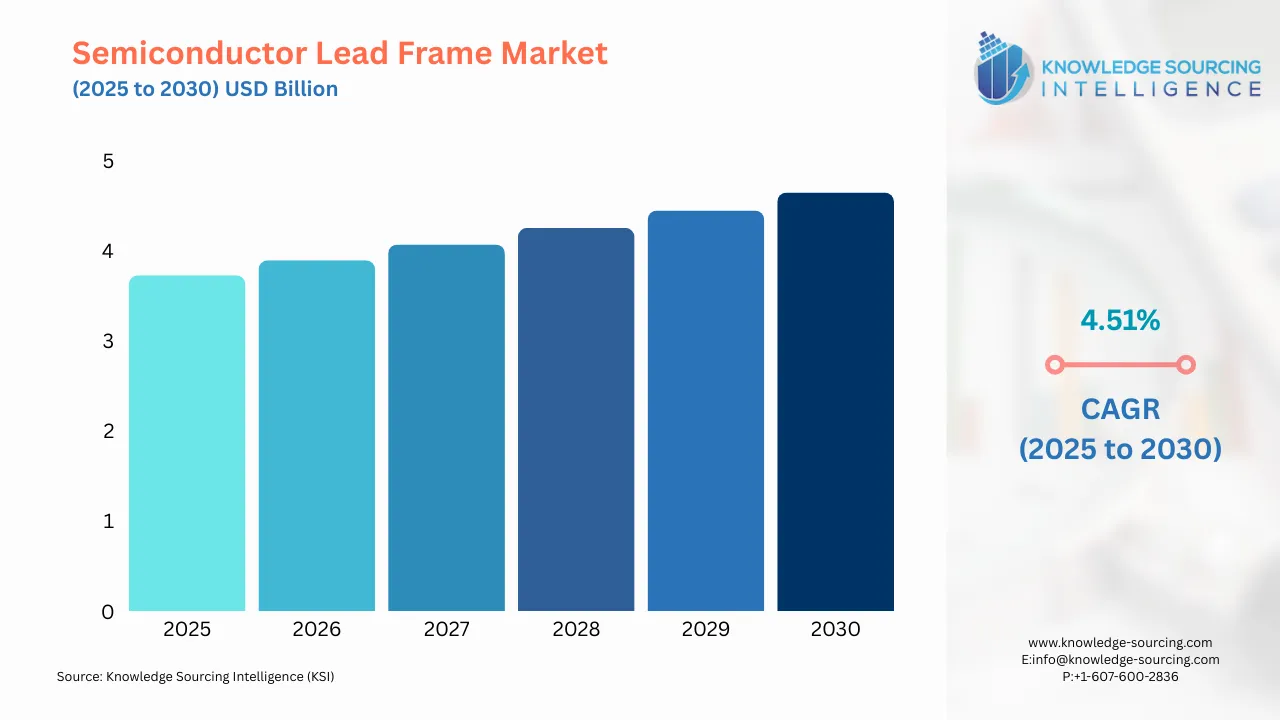
The semiconductor lead frame market is projected to grow at a CAGR of 4.51% to reach US$4.646 billion by 2030, up from US$3.726 billion in 2025.
Highlights:
- 1Increasing electronics demandis driving growth in the semiconductor lead frame market.
- 2Growing miniaturization trendsare boosting the need for precise, compact lead frames.
- 3Asia Pacificis leading the lead frame market with robust semiconductor production.
- 4Advancing stamping technologyis enhancing cost-effective lead frame manufacturing processes.
- 5Rising advanced packaging adoptionis fueling demand for high-performance lead frames.
- 6Expanding automotive sectoris increasing the use of lead frames in ICs.
- 7Strengthening semiconductor investmentsare supporting lead frame market expansion globally.
The Semiconductor Lead Frame Market provides the critical, yet often unseen, component within the semiconductor packaging process. Lead frames function as the core structure for supporting the silicon die, providing the essential electrical connection between the chip and the Printed Circuit Board (PCB), and efficiently dissipating heat from the device. This market’s fundamental activity is intrinsically tied to the overall health and technological trajectory of the global semiconductor industry, particularly the demand for discrete devices and Integrated Circuits (ICs). Market trend is shifting from generic, standard packages toward highly customized, high-reliability lead frames that meet the stringent requirements for superior thermal management and electrical performance in power-intensive applications, which dictates the competitive strategy and investment landscape for manufacturers.
Semiconductor Lead Frame Market Analysis
Growth Drivers
The explosive growth in electric vehicle (EV) production globally creates a non-negotiable demand for high-power semiconductor devices, such as MOSFETs and IGBTs, which rely on thermally efficient lead frames for optimal performance. This shift drives demand for specialized, thick-gauge Copper Alloy lead frames capable of superior heat dissipation. Concurrently, the pervasive rollout of 5G network infrastructure and the corresponding proliferation of IoT devices necessitates the miniaturization of electronic components. This trend mandates the use of fine-pitch, complex-geometry lead frames, directly elevating demand for Chemical Etching processes and advanced QFN (Quad Flat Non-lead) package designs to achieve high-density packaging solutions.
Challenges and Opportunities
The primary market constraint stems from the historically volatile and often rising prices of key raw materials, predominantly Copper Alloys, which compress manufacturer profit margins and complicate long-term pricing strategies for commodity lead frames. A significant opportunity, however, resides in the accelerating global shift toward advanced packaging technologies, including System-in-Package (SiP) and heterogeneous integration. This technological evolution increases the complexity and value-add of the lead frame, driving demand for innovative, custom-engineered designs and advanced surface treatments that offer improved mechanical strength and reliability, moving production away from high-volume, low-margin stamping toward specialized etching.
Raw Material and Pricing Analysis
The semiconductor lead frame is a physical product, with raw materials costs forming a significant portion of the total manufacturing expense. Copper Alloys (e.g., C194, C7025) are the dominant material, accounting for the majority of volume due to their high electrical and thermal conductivity. Iron-Nickel Alloys (e.g., Alloy 42) serve specialized applications requiring low thermal expansion, though in lower volumes. Pricing is heavily influenced by the global commodity market price of copper, which has exhibited volatility exceeding 20% in recent periods due to geopolitical tensions and supply chain bottlenecks. This instability directly impacts the input costs for lead frame manufacturers, making cost-plus pricing mechanisms a necessary, yet challenging, component of sales agreements.
Supply Chain Analysis
The lead frame supply chain is linear and highly concentrated, beginning with the smelting and rolling of copper and iron-nickel alloys, primarily in Asia. Fabrication, involving stamping or chemical etching, is clustered in manufacturing hubs across the Asia Pacific, particularly South Korea, Japan, Taiwan, and China. This geographical concentration creates logistical dependencies, especially for time-sensitive deliveries to downstream Assembly, Test, and Packaging (ATP) houses, which are also highly clustered in these same regions. The complexity lies in managing the high-precision processing and maintaining material quality consistency across global sites, as the final product must meet extremely tight dimensional tolerances for automated wire bonding and molding processes.
Government Regulations:
Jurisdiction | Key Regulation / Agency | Market Impact Analysis |
United States | CHIPS and Science Act (2022) | The Act provides substantial incentives for the domestic manufacturing of semiconductors and associated components. This directly encourages lead frame producers to establish or expand production capacity within the US, creating new domestic market demand and shifting a portion of the global supply chain toward North America. |
European Union | Restriction of Hazardous Substances (RoHS) Directive | The RoHS directive restricts the use of specific hazardous materials, notably lead, in electronic equipment. This compels lead frame manufacturers to continuously invest in R&D for lead-free plating processes (e.g., silver, palladium, or specialized alloys) and new raw material compositions, directly driving demand for compliant, higher-cost, and more complex materials. |
China | Made in China 2025 (Semiconductor Focus) | The policy aims to increase domestic self-sufficiency in core semiconductor components. This fuels government and private investment in local lead frame production facilities and technology development, dramatically increasing domestic production capacity and simultaneously accelerating local market demand from indigenous assembly houses. |
Semiconductor Lead Frame Market Segment Analysis
By Application: Integrated Circuit (IC)
The Integrated Circuit (IC) application segment is the largest consumer of semiconductor lead frames, serving as the foundational platform for logic, memory, and analog chips used across consumer electronics, computing, and telecommunications. Two macro trends fundamentally drive the demand for IC lead frames: increasing unit volumes and relentless miniaturization. The mass-market adoption of smartphones, wearable devices, and laptops dictates massive, continuous volume demand, predominantly for cost-effective stamped lead frames in packages like SOP (Small Outline Package) and QFP (Quad Flat Package). Conversely, the shift to high-performance ICs for 5G modems and advanced microcontrollers necessitates ultra-fine pitch and high pin-count designs, driving demand for the more complex and precise Chemical Etching process to manufacture QFN (Quad Flat Non-lead) packages. The segment’s growth is directly coupled with the silicon content per electronic device, which is consistently increasing due to feature enrichment and connectivity requirements.
By End-Use Industry: Automotive
The Automotive sector is the most significant growth catalyst for high-reliability and high-power lead frames. This necessity is categorically driven by the global transition to Electric Vehicles (EVs) and the proliferation of Advanced Driver-Assistance Systems (ADAS). EV power conversion requires robust, specialized Discrete Devices (IGBTs and MOSFETs) in power modules, which necessitate lead frames fabricated from high-thermal-conductivity Copper Alloys with sophisticated geometries for superior heat dissipation. Lead frames in this segment must comply with stringent quality standards like AEC-Q100, which inherently demands higher manufacturing precision and material integrity compared to consumer-grade electronics. The growth of ADAS and in-car connectivity further increases the number of sensors and microcontrollers, requiring specialized, reliable lead frames that can withstand the harsh thermal and vibrational environments of modern automobiles, thereby creating a premium, non-cyclical demand floor.
Semiconductor Lead Frame Market Geographical Analysis
US Market Analysis
The US market for semiconductor lead frames is characterized by a strong emphasis on high-mix, low-volume, high-value applications, particularly for the Aerospace, Defense, and high-reliability Automotive electronics sectors. Local demand is being directly influenced by the CHIPS Act, which mandates and funds the onshoring of semiconductor manufacturing, thereby initiating new localized demand for domestic lead frame supply. Key factors include stringent military and space-grade specifications, which favor advanced etching and specialized Iron-Nickel alloys over standard copper alloys, creating a premium-priced market for high-specification products.
Brazil Market Analysis
The Brazilian market profile is focused primarily on the domestic assembly operations serving the local Consumer Electronics and automotive industries. Demand is volume-sensitive, with a preference for cost-effective lead frames used in standard IC packages and discrete devices. Local factors, including governmental policies aimed at stimulating domestic electronics manufacturing, act as a moderate demand driver. However, the market remains heavily reliant on imported finished lead frames and primary materials from major Asian production centers due to limited local high-precision fabrication capacity.
Germany Market Analysis
The German market is dominated by the sophisticated requirements of the domestic Automotive industry, acting as the primary driver for lead frame demand. Germany's engineering focus mandates the use of high-reliability, thermally robust lead frames for power semiconductors used in high-end electric and hybrid vehicle components. Demand is concentrated on high-specification Copper Alloy lead frames and advanced packaging types, where adherence to rigorous German industrial quality standards (e.g., IATF 16949) is a non-negotiable factor influencing procurement decisions and favoring established, high-quality Asian and European suppliers.
South Korea Market Analysis
South Korea is a major production and consumption hub, driven by the vertically integrated operations of major domestic semiconductor and consumer electronics giants (e.g., Samsung and LG). The demand for lead frames is high-volume, reflecting the massive output of smartphones, memory chips, and automotive components. Local demand drivers include significant, continuous capital expenditure by domestic manufacturers in the advanced packaging sector, which fuels demand for both standard stamped frames and highly advanced, ultra-fine-pitch etched frames for the latest generation of mobile and memory devices.
China Market Analysis
China represents the largest and fastest-growing market for semiconductor lead frames, driven by two simultaneous forces: massive domestic consumer electronics production and the national imperative for semiconductor self-sufficiency. The high volume of Integrated Circuits and Discrete Devices manufactured locally creates overwhelming demand, primarily for cost-competitive, stamped copper alloy lead frames. Government policies supporting domestic fab expansion and the "Made in China 2025" plan actively promote capacity additions within local lead frame suppliers, shifting procurement preference towards domestic sources and intensifying local production-side competition.
Semiconductor Lead Frame Market Competitive Environment and Analysis
The semiconductor lead frame competitive landscape is characterized by a mix of specialized Japanese and Korean precision engineering firms and large, vertically integrated Asian manufacturers. Competition is fundamentally based on three vectors: precision manufacturing capability (especially for fine-pitch etching), cost-efficiency in high-volume stamping, and raw material sourcing leverage. Major players differentiate themselves by focusing on specific high-value segments, such as automotive-grade reliability, or by achieving superior scale in commodity production. The required capital expenditure for high-precision tooling and plating infrastructure serves as a significant barrier to entry, concentrating market share among established, financially robust companies.
Mitsui High-tec Inc.
Mitsui High-tec Inc. is strategically positioned as a leader in ultra-precision metal processing, leveraging this core competency to produce high-quality lead frames. While its business also encompasses motor cores for electric vehicles, its Electronic Parts segment is dedicated to lead frames. The company excels in high-precision stamping and molding technology, which allows it to serve demanding applications like automotive power modules and high-pin-count QFP packages with exceptional reliability. Mitsui High-tec emphasizes technological refinement and aggressive capital investment to increase production capacity and maintain its edge in precision, as evidenced by a consistent focus on capital investment in its official financial summaries.
Toppan Printing Co., Ltd.
Toppan Printing Co., Ltd. operates a diversified business, with its Electronics segment covering advanced components including lead frames. Toppan leverages its core microfabrication and surface treatment technologies, originally developed for the printing industry, to produce highly precise lead frames. The company is actively focused on lead frames requiring superior surface finishes and complex patterns, often supplying products for high-density ICs and specialized discrete devices. Toppan's strength lies in integrating its manufacturing process with its broader electronics offerings, allowing it to provide a more comprehensive packaging solution to customers.
Haesung DS Co., Ltd.
Haesung DS Co., Ltd. is a specialized supplier of semiconductor materials, with lead frames and package substrates as its primary product lines. The company offers a comprehensive range of lead frame types, including QFN, QFP, and specialized discrete packages, utilizing both etching and stamping processes. Haesung DS specifically targets the high-reliability segment, offering surface treatment solutions like µ-PPF™, which enhance mold adhesion and meet rigorous standards like AEC-Q100 Grade 0, positioning itself as a reliable supplier for the growing automotive and industrial end-use markets.
Semiconductor Lead Frame Market Developments
September 2025: Mitsubishi Electric unveiled its new “Compact DIPIPM” power module series, reducing module footprint to ~53% of prior versions, enabling more compact inverter substrates and creating demand pressure for smaller, denser lead-frame / substrate components.
April 2025: Shinko Electric Industries earned Intel’s 2025 EPIC Supplier Award for excellence in substrate technology, cost, and scale, reinforcing its position as a key lead-frame and packaging-component supplier for major chipmakers.
July 2025: Shinko Electric Industries also acquired the standard certification IATF 16949 for its flip-chip type package manufacturing operations, a quality / automotive-grade credential likely to boost trust and demand for its lead-frame / package output in automotive and high-reliability segments.
Semiconductor Lead Frame Market Scope:
| Report Metric | Details |
|---|---|
| Total Market Size in 2026 | USD 3.726 billion |
| Total Market Size in 2031 | USD 4.646 billion |
| Growth Rate | 4.51% |
| Study Period | 2021 to 2031 |
| Historical Data | 2021 to 2024 |
| Base Year | 2025 |
| Forecast Period | 2026 – 2031 |
| Segmentation | Technology, Material, Application, Geography |
| Geographical Segmentation | Americas, Europe Middle East and Africa (EMEA), Asia Pacific |
| Companies |
|
Semiconductor Lead Frame Market Segmentation:
By Technology
Chemical Etching
Stamping
By Material
Copper Alloys
Iron-Nickel Alloys
Others
By Application
Integrated Circuit (IC)
Discrete Devices
Others
By End-Use Industry:
Automotive
Consumer Electronics
Industrial
Telecommunications
Others
By Geography
Americas
US
Europe, Middle East, and Africa
Germany
Netherland
Others
Asia Pacific
China
Japan
Taiwan
South Korea
Others
Market Segmentation
By Technology
By Material
By Application
By End-users
By Geography
Table of Contents
1. EXECUTIVE SUMMARY
2. MARKET SNAPSHOT
2.1. Market Overview
2.2. Market Definition
2.3. Scope of the Study
2.4. Market Segmentation
3. BUSINESS LANDSCAPE
3.1. Market Drivers
3.2. Market Restraints
3.3. Market Opportunities
3.4. Porter’s Five Forces Analysis
3.5. Industry Value Chain Analysis
3.6. Policies and Regulations
3.7. Strategic Recommendations
4. TECHNOLOGICAL OUTLOOK
5. SEMICONDUCTOR LEAD FRAME MARKET BY TECHNOLOGY
5.1. Introduction
5.2. Chemical Etching
5.3. Stamping
6. SEMICONDUCTOR LEAD FRAME MARKET BY MATERIAL
6.1. Introduction
6.2. Copper Alloys
6.3. Iron-Nickel Alloys
6.4. Others
7. SEMICONDUCTOR LEAD FRAME MARKET BY APPLICATION
7.1. Introduction
7.2. Integrated Circuit (IC)
7.3. Discrete Devices
7.4. Power Electronics
7.5. Others
8. SEMICONDUCTOR LEAD FRAME MARKET BY END-USERS
8.1. Introduction
8.2. Automotive
8.3. Consumer Electronics
8.4. Industrial
8.5. Telecommunications
8.6. Others
9. SEMICONDUCTOR LEAD FRAME MARKET BY GEOGRAPHY
9.1. Introduction
9.2. Americas
9.2.1. United States
9.3. Europe, the Middle East, and Africa
9.3.1. Germany
9.3.2. Netherlands
9.3.3. Others
9.4. Asia Pacific
9.4.1. China
9.4.2. Japan
9.4.3. Taiwan
9.4.4. South Korea
9.4.5. Others
10. COMPETITIVE ENVIRONMENT AND ANALYSIS
10.1. Major Players and Strategy Analysis
10.2. Market Share Analysis
10.3. Mergers, Acquisitions, Agreements, and Collaborations
10.4. Competitive Dashboard
11. COMPANY PROFILES
11.1. Toppan Printing Co., Ltd.
11.2. Mitsui High-tec Inc.
11.3. Shinko Electric Industries Co., Ltd.
11.4. Advanced Assembly Materials International Limited
11.5. ASM Pacific Technology Ltd.
11.6. Chang Wah Technology Co, Ltd.
11.7. Samsung Electronics Co., Ltd. (Semiconductor Business)
11.8. Toshiba Corporation
11.9. Rohm Co., Ltd. (Mechatech Division)
11.10. Haesung DS Co., Ltd.
12. APPENDIX
12.1. Currency
12.2. Assumptions
12.3. Base and Forecast Years Timeline
12.4. Key benefits for the stakeholders
12.5. Research Methodology
12.6. Abbreviations
LIST OF FIGURES
LIST OF TABLES
Navigate
Trusted by the world's leading organizations


