Semiconductor Manufacturing Material Market Share by Material Type, 2025
The semiconductor materials market in 2025 reflects a clear shift from traditional wafer-centric manufacturing to a packaging- and integration-led value chain, with packaging materials emerging as the dominant segment. Growth is increasingly being driven by AI adoption, need for advanced chipsets, and advanced nodes, which are significantly raising material intensity across the production process. While wafers and substrates remain the core, compound semiconductors like SiC and GaN are reshaping demand dynamics. Overall, the market is evolving into a complexity-driven ecosystem where performance, yield, and integration are driving the success stories of major players.
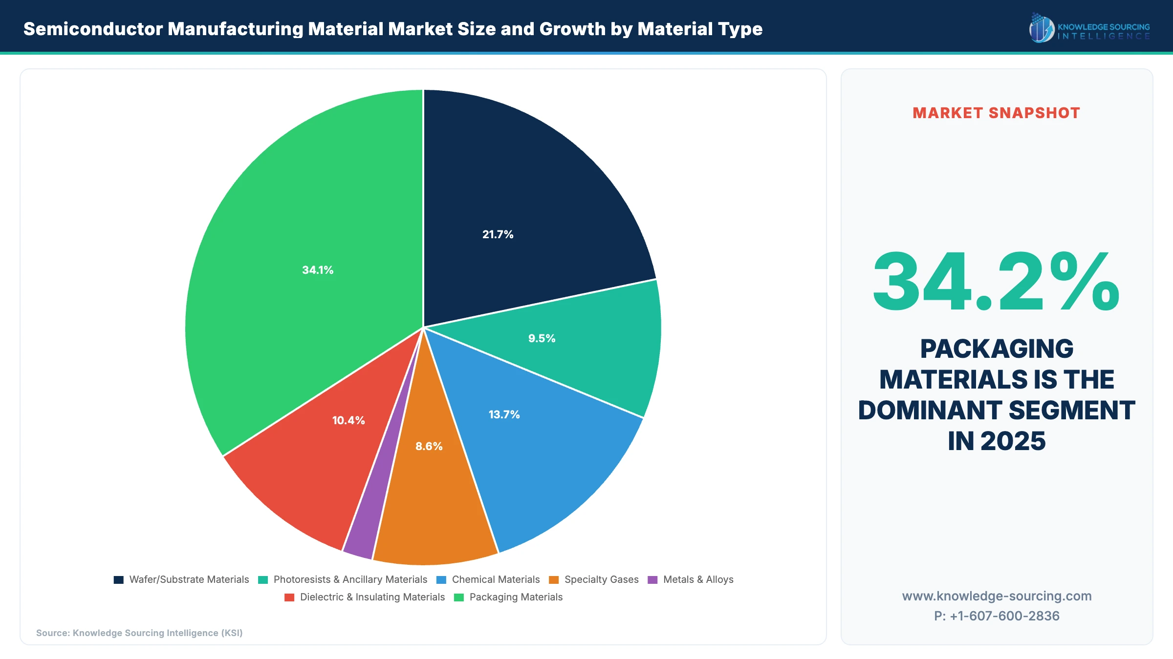 Packaging materials (34.2%) dominance confirms backend is now the primary value capture layer
Packaging has overtaken all other material segments due to the explosion of AI accelerators and chiplet-based architectures.
Advanced packaging (CoWoS, 2.5D/3D IC) used by players like TSMC and Intel is driving disproportionate material intensity per chip.
High-bandwidth memory (HBM) integration is increasing demand for substrates, underfills, and encapsulation materials.
Wafer/Substrate materials (21.8%) growth is increasingly driven by compound semiconductors, not silicon alone
EV power electronics and renewable infrastructure are accelerating adoption of SiC wafers (notably by Wolfspeed).
RF and 5G infrastructure is supporting GaN substrate demand.
Capacity expansions (200mm ? 300mm SiC transition) are raising ASPs structurally, not just volumes.
Chemicals (13.7%) + Specialty gases (8.6%) scale with process complexity, creating supply chain leverage points
Advanced nodes (5nm, 3nm) require more etch, deposition, and cleaning cycles per wafer.
Rare gases (neon, xenon) and ultra-high purity chemicals have become geopolitically sensitive inputs.
Supply disruptions (e.g., Ukraine-origin neon) have forced fabs to vertically secure material sourcing.
Photoresists & ancillaries (9.5%) are tightly coupled to EUV adoption and yield economics
EUV lithography adoption by ASML customers is driving demand for next-gen chemically amplified resists.
Each additional EUV layer increases defect sensitivity, raising the need for high-performance ancillary materials.
Yield improvement is the primary growth driver.
Dielectrics (10.4%) vs Metals & Alloys (2.1%) highlights transistor architecture transition
Transition from FinFET to Gate-All-Around (GAA) architectures increases reliance on high-k dielectrics for electrostatic control.
Interconnect scaling challenges are pushing innovation in low-k materials to reduce RC delay.
Metals remain essential but are process-optimized commodities with limited differentiation.
By Material Type | 2024 | 2025 | 2030 | CAGR (25-30) |
Wafer/Substrate Materials | 15.008 | 15.650 | 17.750 | 2.55% |
Photoresists & Ancillary Materials | 6.092 | 6.794 | 10.472 | 9.04% |
Chemical Materials | 9.416 | 9.813 | 11.094 | 2.48% |
Specialty Gases | 5.752 | 6.147 | 7.899 | 5.14% |
Metals & Alloys | 1.397 | 1.474 | 1.775 | 3.79% |
Dielectric & Insulating Materials | 7.163 | 7.459 | 8.387 | 2.37% |
Packaging Materials | 23.007 | 24.554 | 31.373 | 5.02% |
Source: Knowledge Sourcing Intelligence (KSI)
Want deeper insights? Get the full market report.
Access complete market analysis, data tables, and strategic forecasts for:
Semiconductor Manufacturing Material Market - Strategic Insights and Forecasts (2025-2030)
Get in Touch
Interested in this topic? Contact our analysts for more details.