Report Overview
Dielectric Etchers Market Size:
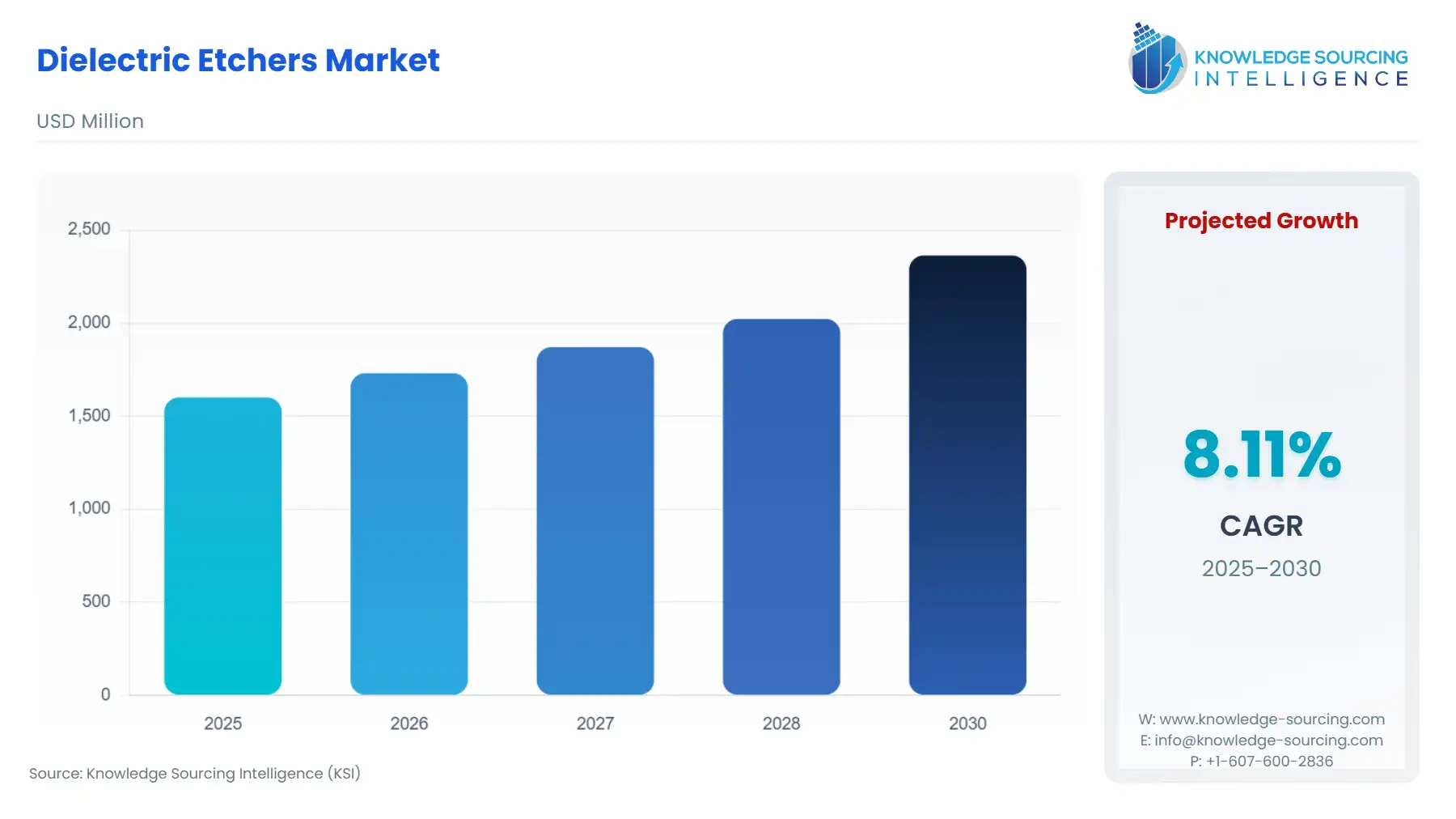
The dielectric etchers market, with a 8.10% CAGR, is anticipated to reach USD 2.364 billion in 2030 from USD 1.601 billion in 2025.
Highlights:
- 1Advanced-node scaling and 3D NAND growth are driving strong demand for high-precision etchers such as cryogenic and high-aspect-ratio systems.
- 2Regulatory pressures, including export controls and fluorinated-gas emissions, are reshaping procurement strategies and favoring low-GWP, abatement-ready tools.
- 3Capital investments under public incentive programs (e.g., CHIPS) are boosting tool demand by enabling fab expansions and upgrades.
- 4Recent product launches — notably by Lam Research, Applied Materials, and Tokyo Electron — reflect OEMs’ focus on deeper, faster, and cleaner dielectric etch processes.
Dielectrics etch systems are central to modern semiconductor manufacturing, particularly for logic memory and advanced packaging. The push toward higher layer-count 3D NAND, tighter feature control, and more stringent environmental requirements have elevated the importance of etch tools. OEMs are racing to supply platforms that deliver both performance and compliance, while fab operators increasingly weigh total cost of ownership (TCO), throughput, and sustainability when selecting new etch equipment.
Dielectric Etchers Market Analysis
- Growth Drivers
Demand is primarily propelled by the rapid scaling of 3D NAND memory. As manufacturers pursue ever-higher layer counts, there is increased need for etch systems capable of creating very deep, narrow channels with atomic-level precision; cryogenic etch technologies directly address this need. Logic fabs also drive demand: shrinking features in the angstrom era demand tighter critical-dimension (CD) control and more complex pattern shaping, which in turn require advanced dielectric etch platforms. Finally, government-led semiconductor funding initiatives accelerate capex cycles, creating fresh demand for etching equipment as new fabrication sites come online or existing fabs expand.
- Challenges and Opportunities
The U.S. tariff environment continues to exert a nuanced but material influence on the dielectric etchers market, mainly through its direct effect on import costs, supply-chain structuring, and competitive dynamics between domestic and Asia-Pacific manufacturing hubs. Dielectric etchers imported under HTS 8486 classifications typically enter the U.S. with zero basic duty, and semiconductor-production equipment has periodically been exempted from additional punitive duties, providing essential tariff stability for fabs and OEMs. However, the persistent risk of policy fluctuations—particularly around China-origin semiconductor equipment—creates a volatile cost environment for global suppliers.
On the challenge side, regulatory and export-control restrictions restrict some tool flows, particularly for sensitive advanced equipment, which can delay customer orders or force OEMs to build compliant variants. Also, environmental regulations on fluorinated gases impose higher costs for both tool manufacturers and chipmakers, pressuring margins. However, these constraints open opportunity: OEMs that can deliver low-GWP etch chemistries, integrated abatement, or retrofit solutions can gain share. Furthermore, equipment providers who partner with fabs under public incentive schemes (such as national semiconductor programs) are well-positioned to capture demand from newly subsidized capacity.
- Raw Material and Pricing Analysis
Key inputs for dielectric etchers include specialty gases (such as fluorinated etch gases), RF power components, vacuum systems, and precision plasma-chamber parts. As regulators increasingly scrutinize high-global-warming-potential (GWP) gases, costs for gas supply and abatement infrastructure are rising. Tool makers may absorb part of these costs or embed abatement systems to maintain customer competitiveness. Higher raw-material and compliance costs can contribute to a higher total cost of ownership, especially for legacy fabs that operate on tighter margins and may delay upgrades.
- Supply Chain Analysis
Dielectric etcher manufacturing is concentrated in advanced equipment hubs across the US, Japan, and Europe, with critical subcomponents (e.g., RF power supplies, mass-flow controllers) sourced globally. Export-control regimes impose routing risk and lead-time variability, especially to restricted jurisdictions. Logistical complexity includes not just hardware delivery but also installation, calibration, and post-install validation in clean-room environments. Companies that maintain strong local service networks and domestic spares inventory enjoy an advantage because they minimize downtime and reduce procurement cycle risk.
Dielectric Etchers Market Government Regulations
|
Jurisdiction |
Key Regulation / Agency |
Market Impact Analysis |
|
United States |
Export licensing, BIS (Bureau of Industry and Security) |
Tight export rules restrict the destinations for advanced dielectric etchers, increasing compliance overhead and potentially slowing orders into restricted markets. |
|
European Union |
PFAS / fluorinated-gas regulation, chemical emissions guidance |
Stricter environmental rules push fabs to demand low-GWP gas chemistries or integrated abatement modules, influencing tool specification and TCO. |
|
Japan |
Export control under METI (Ministry of Economy, Trade and Industry) |
Licensing can limit tool exports; OEMs must navigate regulatory review when shipping advanced etch systems produced in Japan. |
Dielectric Etchers Market Segment Analysis
- Reactive Ion Etching (RIE) — By Technology
Reactive Ion Etching (RIE) remains foundational to dielectric etching, combining ion bombardment with reactive chemistries to deliver highly anisotropic profiles. Its importance is magnified in advanced logic and memory fabs: as devices shrink, RIE systems must deliver extremely precise CD control, low line-edge roughness, and uniformity across the wafer. Moreover, for 3D NAND, RIE variants (and hybrid cryo-RIE flows) are required to etch high aspect ratio features with minimal damage. Regulatory pressure around fluorinated gas use also makes gas-efficient, abatement-enabled RIE tools more attractive. Because RIE tools are deeply embedded in both front-end wafer patterning flows and MEMS or interconnect processes, improvements in RIE performance or efficiency directly influence replacement cycles and incremental purchases in high-volume fabs.
- Electronica — By End-User Industry
The “Electronica” end-user segment, covering high-volume computing, communications, and consumer devices, represents the largest demand base for dielectric etchers. Consumer electronics manufacturers drive wafer volume through continuous refresh cycles, while datacenter operators push memory capacity for AI workloads, increasing 3D NAND demand. The rapid pace of innovation compels semiconductor customers to upgrade etch tools for better profiles, throughput, and lower emissions. Moreover, the growth of edge AI and high-bandwidth memory creates demand for deeply scaled memory and interconnects, further driving etch intensity. Public incentives and geopolitical shifts encourage local fab builds, allowing electronics OEMs to influence etch tool sourcing more directly and stimulating procurement in new regions.
Dielectric Etchers Market Geographical Analysis
- United States
The U.S. market benefits from robust public investment (e.g., CHIPS-style subsidies) for onshore fab capacity. These investments drive demand for dielectric etchers as new 3D NAND and logic capacity is built domestically. Additionally, export-control compliance requirements add complexity but also boost demand for domestic tool providers.
- Germany (Europe)
In Germany, stringent environmental regulations (particularly around fluorinated-gas emissions) push fabs toward low-GWP etch technologies. European fabs increasingly demand tools with abatement systems, influencing purchasing decisions and favoring tool vendors who can meet the regulatory and sustainability bar.
- Japan
Japanese fabs and OEMs are deeply integrated into the global etch supply chain. Japan’s export-control policies influence where advanced systems can be sold, and domestic capital investments support continuous tool development. OEMs headquartered in Japan benefit from proximity to leading-edge fabs and local service capabilities.
- South Korea
Large-scale memory manufacturers in South Korea significantly shape global demand. However, the alignment of Korean export policy with allied countries influences the timing of tool procurements. Local demand is also driven by the need to maintain global competitiveness in memory density and performance.
- Taiwan
Taiwan’s advanced foundries are key buyers of dielectric etch equipment. Proposed tightening of export-control measures complicates procurement logistics. Nevertheless, Taiwan remains a major market for high-aspect-ratio and cryogenic etch systems as local fabs invest in next-generation 3D NAND scaling.
Dielectric Etchers Market Competitive Environment and Analysis
Major players in the dielectric etchers market include Lam Research, Applied Materials, Tokyo Electron, Oxford Instruments, ULVAC, Mattson Technology, Hitachi High-Tech, and SPTS. These firms differentiate by throughput, yield, environmental performance, and local service.
- Lam Research is a front-runner in cryogenic dielectric etching. Its Cryo 3.0 technology enables very deep, high-aspect-ratio memory channel etch with angstrom-level precision, while delivering higher throughput and significantly lower emissions. Lam’s Cryo 3.0 also integrates with its Vantex and Flex platforms, maximizing performance and capital reuse.
- Applied Materials competes via a broadened patterning portfolio. It introduced a new etch system (Sym3 Y Magnum) that deposits and etches within a single chamber to smooth line-edge roughness after EUV and launched a CVD patterning film designed for angstrom-era scaling. These innovations help customers reduce defectivity and cost in advanced nodes.
- Tokyo Electron is advancing in ultra-fine pattern shaping with its Acrevia™ gas cluster beam (GCB) system — a low-damage approach to correct EUV-printed features, improve yield, and support tighter geometries.
Dielectric Etchers Market Developments
- July 2024: Lam Research launched its Cryo 3.0 cryogenic dielectric etch technology, capable of etching highly vertical, high-aspect-ratio structures at high speed with double the etch rate of conventional processes.
- July 2024: Tokyo Electron introduced its Acrevia™ gas cluster beam system, which enables precise sidewall modification, reduces line-edge roughness, and corrects pattern defects post-EUV lithography.
- February 2024: Applied Materials expanded its patterning solutions portfolio by introducing the Sym3 Y Magnum etch system and a new CVD patterning film; the offerings are designed to address challenges at 2 nm and below, improving yield and reducing patterning complexity.
Dielectric Etchers Market Segmentation:
BY TYPE
- Wet etching
- Dry etching
- Atomic-level etching
- Reactive ion etching
BY APPLICATION
- Semiconductor Manufacturing
- MEMS
- Optoelectronics
- Power Devices
BY END-USER INDUSTRY
- Electronica
- Automotive
- Aerospace & Defense
- Medical Devices
By Geography
- North America
- United States
- Canada
- Mexico
- South America
- Brazil
- Argentina
- Others
- Europe
- Germany
- France
- United Kingdom
- Spain
- Others
- Middle East and Africa
- Saudi Arabia
- UAE
- Others
- Asia Pacific
- China
- India
- South Korea
- Taiwan
- Thailand
- Indonesia
- Japan
- Others
Market Segmentation
By Type
By Application
By End-user Industry
By Geography
Table of Contents
1. EXECUTIVE SUMMARY
2. MARKET SNAPSHOT
2.1. Market Overview
2.2. Market Definition
2.3. Scope of the Study
2.4. Market Segmentation
3. BUSINESS LANDSCAPE
3.1. Market Drivers
3.2. Market Restraints
3.3. Market Opportunities
3.4. Porter’s Five Forces Analysis
3.5. Industry Value Chain Analysis
3.6. Policies and Regulations
3.7. Strategic Recommendations
4. TECHNOLOGICAL OUTLOOK
5. Dielectric Etchers Market BY Type
5.3. Dry etching
5.4. Atomic-level etching
5.5. Reactive ion etching
6. Dielectric Etchers Market BY Application
6.1. Introduction
6.2. Semiconductor Manufacturing
6.3. MEMS
6.4. Optoelectronics
6.5. Power Devices
7. Dielectric Etchers Market BY End-User INDUSTRY
7.1. Introduction
7.2. Electronics
7.3. Automotive
7.4. Aerospace & Defense
7.5. Medical Devices
8. Dielectric Etchers Market BY GEOGRAPHY
8.1. Introduction
8.2. North America
8.2.1. By Type
8.2.2. By Application
8.2.3. By End-User Industry
8.2.4. By Country
8.2.4.1. United States
8.2.4.2. Canada
8.2.4.3. Mexico
8.3. South America
8.3.1. By Type
8.3.2. By Application
8.3.3. By End-User Industry
8.3.4. By Country
8.3.4.1. Brazil
8.3.4.2. Argentina
8.3.4.3. Others
8.4. Europe
8.4.1. By Type
8.4.2. By Application
8.4.3. By End-User Industry
8.4.4. By Country
8.4.4.1. United Kingdom
8.4.4.2. Germany
8.4.4.3. France
8.4.4.4. Italy
8.4.4.5. Spain
8.4.4.6. Others
8.5. Middle East & Africa
8.5.1. By Type
8.5.2. By Application
8.5.3. By End-User Industry
8.5.4. By Country
8.5.4.1. Saudi Arabia
8.5.4.2. UAE
8.5.4.3. Others
8.6. Asia Pacific
8.6.1. By Type
8.6.2. By Application
8.6.3. By End-User Industry
8.6.4. By Country
8.6.4.1. Japan
8.6.4.2. China
8.6.4.3. India
8.6.4.4. South Korea
8.6.4.5. Taiwan
8.6.4.6. Indonesia
8.6.4.7. Thailand
8.6.4.8. Others
9. COMPETITIVE ENVIRONMENT AND ANALYSIS
9.1. Major Players and Strategy Analysis
9.2. Market Share Analysis
9.3. Mergers, Acquisitions, Agreements, and Collaborations
9.4. Competitive Dashboard
10. COMPANY PROFILES
10.1. Lam Research Corporation
10.2. Hitachi High-technologies Corporation
10.3. Mattson Technology Inc
10.4. Tokyo Electron
10.5. Oxford Instruments
10.6. ULVAC Inc
10.7. Applied Materials Inc
10.8. SPTS Technology
11. RESEARCH METHODOLOGY
LIST OF FIGURES
LIST OF TABLES
Navigate
Trusted by the world's leading organizations


