Report Overview
Semiconductor Etch Equipment Market Size:
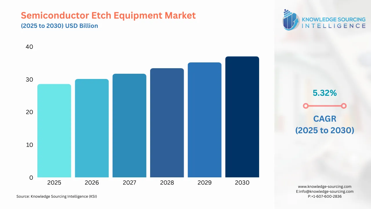
The Semiconductor Etch Equipment Market is expected to grow from USD 28.578 billion in 2025 to USD 37.024 billion in 2030, at a CAGR of 5.32%.
Semiconductor Etch Equipment Market Overview:
Etching is a critical operation in the semiconductor production cycle. This method removes material from the surface of the semiconductor to form patterns depending on its applications. The expansion of the semiconductor wafer deposition and wafer processing industries is critical to the semiconductor etch equipment market growth. An increased emphasis on consumer electronics is one of the key factors driving market expansion. Furthermore, industrial automation, continual developments in consumer electronics, and the use of vehicle sensors are expanding the applications of semiconductors. Their popularity in practically all industrial verticals contributes to the market's expansion.
Semiconductor Etch Equipment Market Growth Drivers:
The rise in innovation in the consumer electronics market is paving the way for company-wide cooperation on new etch technology.
In recent years, IoT and 5G gadgets have become quicker, smaller, and more multifunctional. This has given rise to advanced packaging technology-based production, in which a middle-end process has been inserted between the front-end and back-end processes in semiconductor manufacturing. As a result, in October 2019, IBM Japan, Ltd. and Panasonic Corporation's subsidiary, Panasonic Smart Factory Solutions Co., Ltd., announced a collaboration to develop and market a new high-value-added system to optimize the overall equipment effectiveness (OEE) of customers' semiconductor manufacturing processes and achieve high-quality manufacturing. Panasonic is currently developing and marketing cutting-edge equipment and manufacturing methods that aid in the advancement of semiconductor production for advanced packaging. New gadgets and procedures include dry etching equipment, plasma dicers to manufacture high-quality wafers, plasma cleaners to boost metal and resin adherence, and high-accuracy bonding devices. This experience will be integrated with techniques and technology created by IBM Japan for semiconductor production to assist Panasonic in developing smart factory technology.
Semiconductor Etch Equipment Market Segmentation Analysis:
The introduction of plasma etching technology will drive significant growth in the high-density etch equipment category.
Plasma etching is a vital procedure used in semiconductor manufacture to remove materials from unit surfaces, and it is the only economically feasible method for anisotropic surface removal. As the semiconductor industry strives to lower crucial feature sizes and increase device performance, etch processing problems are increasing as smaller features are treated with novel device designs. Higher density and aspect ratio features present new issues requiring extra innovation in various wafer processing areas. Because of their complexity, these developments rely increasingly on detailed physical, chemical, and computational models of plasma etch processes. For instance, Lam Research Corporation announced the launch of a completely transformed plasma etch technology and system solution in March 2020. According to the company, this technology is intended to give chipmakers with advanced functionality and extendibility needed for future innovation. As per the same source, Lam's Sense.i platform provides unrivalled system intelligence in a compact, high-density architecture to enable process performance at the highest productivity, enabling logic and memory device roadmaps for the next decade.
The miniaturization of semiconductors necessitates the use of advanced etching technologies, such as conductor etching equipment.
Conductor etching equipment is commonly used to form the electrically active materials found in various portions of a semiconductor device. Even little variations in these microscopic semiconductor structures can result in an electrical fault that degrades device performance. During the forecasted period, the increasing demand for downsizing semiconductor circuits is expected to stimulate the ever-increasing demand for various types of conductors etching equipment and the necessity for high production of multi-film stacks with tiny faults. For example, Applied Materials, Inc. announced in August 2020 a new addition to its very successful Centris Sym3 etch product line, allowing chipmakers to accurately pattern and shape ever-smaller features in cutting-edge memory and logic devices. It employs cutting-edge RF pulsing technology to enable clients to produce densely packed, high-aspect-ratio structures in 3D NAND, DRAM, and logic, including FinFETs and upcoming gate-all-around architectures, by providing exceptionally high materials selectivity, depth control, and profile control.
Semiconductor Etch Equipment Market Geographical Outlook:
The Asia Pacific region is estimated to have the fastest growth rate.
The Asia-Pacific region accounts for the lion's share of worldwide semiconductor foundries. According to a survey by the Semiconductor Sector Association in July 2021, China has mastered various chip technologies, and its commercial semiconductor industry is still very young. Nonetheless, the Chinese government is attempting to bridge the gap by investing an estimated $28.9 billion in October 2019. It is positioned to become more competitive in the semiconductor etch equipment industry due to rising markets. For instance, Advanced Micro-Fabrication Equipment Inc., China (AMEC), celebrated a milestone for its capacitively coupled plasma (CCP) etch systems in November 2021 by shipping its 1500th station to a top Chinese semiconductor manufacturer. AMEC's etcher innovation continues to reinforce the company's position as an equipment leader, boost market share, and fuel growth.
India has also always had a lot of research and development skills and resources. Many of the world's biggest semiconductor and WFE producers and considerable R&D capabilities are based in India. The availability of a technically skilled workforce greatly assists in product design and testing. For instance, Lam Research declared in September 2022 the inauguration of its second research and development (R&D) centre in India. The new centre will feature a "state-of-the-art" hardware engineering lab with deposition, etching, and wet processing devices, as well as AR/VR capabilities.
Semiconductor Etch Equipment Market Key Developments:
October 2025: Applied Materials launched the Centura™ Xtera™ Epi system, integrating pre-clean/etch to enable void-free, uniform epitaxial layers for 2nm Gate-All-Around transistors.
April 2025: Lam Research donated a multi-chamber etch system (including conductor, dielectric & deep-reactive-ion etch chambers) to UC Berkeley’s Marvell Nanofabrication Lab, supporting R&D for next-gen device architectures, specialty semiconductors & nanofabrication.
February 2025: Lam Research unveiled Akara®, its most advanced plasma conductor etch tool, offering new precision control for scaling GAA transistors and 3D NAND devices.
Oct 2024: Tokyo Electron (TEL) reported development of cryogenic etching for 3D NAND, which significantly reduces CO2 emissions (by ~80%) compared to conventional etch, supporting “digital & green transformation” in etch processes.
List of Top Semiconductor Etch Equipment Companies:
Lam Research
Applied Materials
Tokyo Electron Limited
Oxford Instruments
Hitachi High-Tech Corporation
Semiconductor Etch Equipment Market Scope:
| Report Metric | Details |
|---|---|
| Total Market Size in 2025 | USD 28.578 billion |
| Total Market Size in 2030 | USD 37.024 billion |
| Forecast Unit | Billion |
| Growth Rate | 5.32% |
| Study Period | 2020 to 2030 |
| Historical Data | 2020 to 2023 |
| Base Year | 2024 |
| Forecast Period | 2025 – 2030 |
| Segmentation | Equipment Type, Etching Film Type, Application, Geography |
| Geographical Segmentation | North America, South America, Europe, Middle East and Africa, Asia Pacific |
| Companies |
|
Semiconductor Etch Equipment Market Segmentation:
By Equipment Type
High-density Etch Equipment
Low-density Etch Equipment
By Etching Film Type
Conductor Etching
Dielectric Etching
Polysilicon Etching
By Application
Power Device
MEMS
Sensors
Logic and Memory
Others
By Geography
North America
USA
Canada
Mexico
South America
Brazil
Argentina
Others
Europe
UK
Germany
France
Italy
Spain
Others
Middle East and Africa
Saudi Arabia
UAE
Others
Asia Pacific
China
Japan
India
South Korea
Australia
Others
Market Segmentation
By Equipment Type
By Etching Film Type
By Application
By Geography
Table of Contents
1. EXECUTIVE SUMMARY
2. MARKET SNAPSHOT
2.1. Market Overview
2.2. Market Definition
2.3. Scope of the Study
2.4. Market Segmentation
3. BUSINESS LANDSCAPE
3.1. Market Drivers
3.2. Market Restraints
3.3. Market Opportunities
3.4. Porter’s Five Forces Analysis
3.5. Industry Value Chain Analysis
3.6. Policies and Regulations
3.7. Strategic Recommendations
4. TECHNOLOGICAL OUTLOOK
5. SEMICONDUCTOR ETCH EQUIPMENT MARKET BY EQUIPMENT TYPE
5.1. Introduction
5.2. High-density Etch Equipment
5.3. Low-density Etch Equipment
6. SEMICONDUCTOR ETCH EQUIPMENT MARKET BY ETCHING FILM TYPE
6.1. Introduction
6.2. Conductor Etching
6.3. Dielectric Etching
6.4. Polysilicon Etching
7. SEMICONDUCTOR ETCH EQUIPMENT MARKET BY APPLICATION
7.1. Introduction
7.2. Power Device
7.3. MEMS
7.4. Sensors
7.5. Logic and Memory Devices
7.6. Others
8. SEMICONDUCTOR ETCH EQUIPMENT MARKET BY GEOGRAPHY
8.1. Introduction
8.2. North America
8.2.1. USA
8.2.2. Canada
8.2.3. Mexico
8.3. South America
8.3.1. Brazil
8.3.2. Argentina
8.3.3. Others
8.4. Europe
8.4.1. United Kingdom
8.4.2. Germany
8.4.3. France
8.4.4. Italy
8.4.5. Spain
8.4.6. Others
8.5. Middle East & Africa
8.5.1. Saudi Arabia
8.5.2. UAE
8.5.3. Others
8.6. Asia Pacific
8.6.1. Japan
8.6.2. China
8.6.3. India
8.6.4. South Korea
8.6.5. Australia
8.6.6. Others
9. COMPETITIVE ENVIRONMENT AND ANALYSIS
9.1. Major Players and Strategy Analysis
9.2. Market Share Analysis
9.3. Mergers, Acquisitions, Agreements, and Collaborations
9.4. Competitive Dashboard
10. COMPANY PROFILES
10.1. Lam Research
10.2. Applied Materials
10.3. Tokyo Electron Limited
10.4. Oxford Instruments
10.5. Hitachi High-Tech Corporation
10.6. Gigalane
10.7. Amec
10.8. Plasma-Therm LLC
10.9. Panasonic Corporation
10.10. ULVAC, Inc
11. APPENDIX
11.1. Currency
11.2. Assumptions
11.3. Base and Forecast Years Timeline
11.4. Key benefits for the stakeholders
11.5. Research Methodology
11.6. Abbreviations
LIST OF FIGURES
LIST OF TABLES
Semiconductor Etch Equipment Market Report
Trusted by the world's leading organizations


