Report Overview
Memory Packaging Market Size:
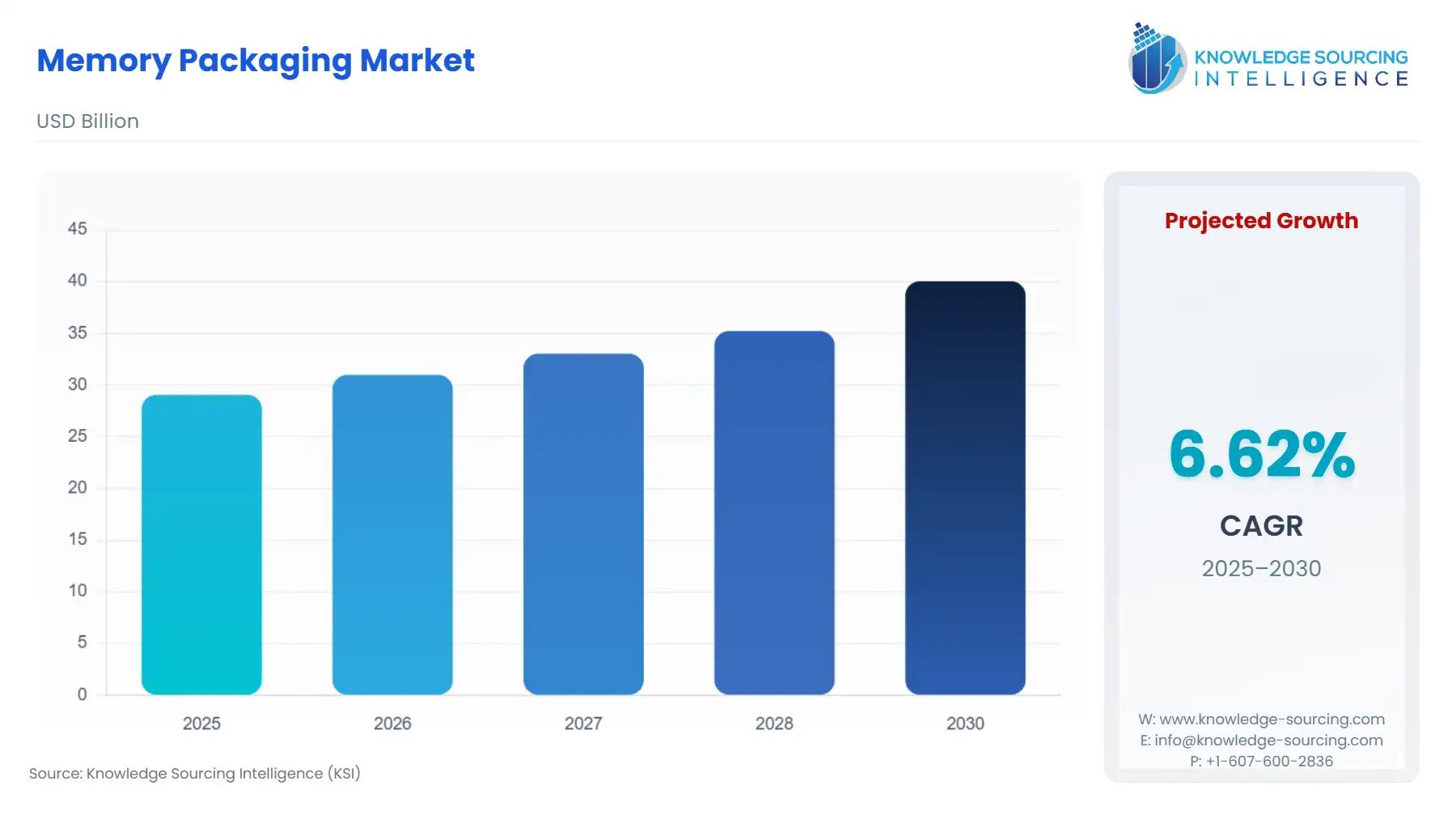
The global memory packaging market, with a 6.62% CAGR, is anticipated to reach USD 40.057 billion in 2030 from USD 29.069 billion in 2025.
Highlights:
- 1CHIPS Act–driven capacity expansion in the United States is accelerating demand for domestic memory packaging and OSAT capabilities.
- 2Wafer-level chip-scale packaging (WLCSP/WLP) and fan-out structures continue to increase package complexity and materials intensity.
- 3Copper, substrate laminates, and specialty dielectrics remain major cost drivers, with pricing affected by concentrated global supply and commodity volatility.
- 4Leading OSATs—including Amkor and ASE—are expanding capacity for advanced memory packaging aligned with AI, automotive, and mobile demand.
Following the highlights, the report provides a demand-centric analysis for industry executives, emphasizing how regulatory actions, materials constraints, and platform-specific technology shifts reshape procurement volumes and packaging mix across global memory supply chains.
Memory Packaging Market Analysis
- Growth Drivers
Three primary forces are expanding demand for memory packaging. Rising AI and high-performance computing workloads require advanced memory formats such as HBM and 2.5D/3D assemblies, increasing TSV processing, substrate routing, and interposer-level packaging demand. National semiconductor policies—including U.S. CHIPS Act incentives and Taiwan industrial support programs—are redirecting procurement toward local and regionally diversified packaging sites, strengthening demand for domestic OSAT capacity. At the consumer level, smartphone, wearable, and IoT OEMs continue to adopt WLCSP formats for NAND and DRAM components to reduce footprint and power consumption. These trends collectively increase total packaging volume, complexity, and tooling investment across the memory supply chain.
- Challenges and Opportunities
The imposition of U.S. tariffs on semiconductor components and outsourced assembly, testing, and packaging (OSAT) services—particularly those originating from China, Taiwan, South Korea, and Malaysia—has created a complex cost and supply-chain environment for the memory packaging market. Higher import duties on substrates, leadframes, advanced packaging materials, and contract packaging services have increased the landed cost of packaged DRAM, NAND, and advanced 2.5D/3D memory modules, pushing manufacturers to reconsider their global sourcing strategies. For U.S.-based semiconductor companies, tariffs are accelerating partial onshoring initiatives, expanding domestic backend assembly operations, and increasing reliance on tariff-exempt regions such as Vietnam and Mexico for redistribution and final assembly.
Cost pressures from copper, substrate laminates, and bonding materials present structural headwinds, with volatility in upstream supply limiting short-term elasticity. Compliance obligations under global chemical restrictions and conflict-mineral regimes add documentation and procurement burdens that can delay supplier qualification. On the opportunity front, government-supported on-shoring initiatives open new volume for domestic OSAT operations, stabilizing demand visibility. Rapid growth in AI accelerators and automotive electronics shifts demand toward high-reliability and high-density memory packages, enabling suppliers with advanced WLP, TSV, and fan-out capabilities to secure long-term contracts. As these segments outpace consumer applications, advanced memory packaging absorbs a larger share of total OSAT utilization.
- Raw Material and Pricing Analysis
Memory packaging relies heavily on copper for leadframes and routing layers, substrate laminates for high-density interconnects, and specialty dielectrics for underfills and encapsulation. Copper price fluctuations and concentrated refining capacity directly influence substrate and leadframe costs. Laminate substrates continue to experience capacity bottlenecks due to limited global manufacturing expansion, resulting in longer lead times and upward pricing pressure. Bonding wire and solder material costs also influence the unit economics of wire bond and WLCSP memory packages. These raw-material constraints raise the cost base for OSATs and push buyers toward longer procurement cycles, with advanced formats absorbing the largest pass-through impact.
- Supply Chain Analysis
Memory packaging supply chains remain centered in Taiwan, South Korea, China, Malaysia, and Vietnam, with robust ecosystems for substrate production, assembly, and final testing. The U.S. and parts of Europe are increasing advanced packaging investment, but high-volume output still relies on Asian hubs. The supply chain features multiple cross-border dependencies: wafers are often fabricated in one country, packaged in another, and tested elsewhere. Substrates and specialty chemicals travel through multi-step logistics routes with limited supplier redundancy. Specialized equipment lead times—particularly for WLP, TSV, and redistribution-layer tools—introduce additional constraints. These interdependencies create sensitivity to regulatory, freight, and geopolitical disruptions.
Memory Packaging Market Government Regulations
|
Jurisdiction |
Key Regulation / Agency |
Market Impact Analysis |
|
United States |
CHIPS and Science Act / Department of Commerce |
Incentivizes domestic advanced packaging plants and increases demand for U.S.-based OSAT capacity, pulling procurement on-shore. |
|
European Union |
RoHS Directive / European Commission |
Requires material substitution and compliance documentation for restricted substances, influencing material qualification and packaging process changes. |
|
Taiwan |
Industrial support programs / Ministry of Economic Affairs |
Strengthens local investment in advanced packaging technologies, sustaining Taiwan’s dominance in memory assembly and test services. |
Memory Packaging Market Segment Analysis
- Wafer Level Chip Scale Packaging (WLCSP/WLP) — Technology
WLCSP executes the entire packaging process at the wafer level, enabling compact, low-profile memory components well suited for mobile, IoT, and wearable applications. Demand stems from OEM requirements for reduced board area, lower power consumption, and improved electrical performance. Multi-die NAND configurations further reinforce the need for efficient wafer-level routing and bumping structures. However, WLCSP introduces technical complexities such as warpage, solder fatigue, and thermal stress, requiring specialized materials and process control. These challenges elevate the value of OSATs capable of achieving low defect densities at high wafer throughput. As OEMs seek proven WLCSP partners, procurement shifts from commodity packaging suppliers toward facilities with advanced wafer-level test, redistribution-layer expertise, and traceability systems. This transition directly increases the number of wafer-level memory packages contracted annually, particularly in mobile-centric markets. The segment’s demand profile favors suppliers with sustained capital investment, as toolsets and metrology requirements exceed those of conventional lead-frame packaging.
- Automotive — End-User
The automotive sector’s requirements for ADAS, infotainment, connectivity, and EV power management generate substantial demand for high-reliability memory packages. Automakers mandate AEC-Q qualification, long-lifecycle sourcing, and strict traceability, shaping their supplier selection criteria. Memory used in braking systems, battery management, and autonomous-driving modules must withstand wide temperature ranges, vibration, and extended service life. These needs drive consistent procurement of automotive-grade DRAM and NAND packages featuring robust underfill materials, high-temperature epoxy systems, and reinforced interconnect structures. In addition, national industrial-policy incentives encourage regional production of automotive electronics, increasing the volume of localized memory packaging orders. Unlike consumer markets, where demand fluctuates with device cycles, automotive contracts lock in multi-year volume commitments, supporting predictable demand for specialized packaging runs. These contracts command premium pricing due to higher qualification costs, metrology requirements, and reliability testing. Overall, automotive remains a critical demand anchor for advanced memory packaging, particularly for suppliers able to meet stringent quality regimes.
Memory Packaging Market Geographical Analysis
- United States
Federal incentives for domestic semiconductor manufacturing, particularly for assembly and test, are increasing procurement toward U.S.-based advanced packaging. Automakers, defense contractors, and cloud operators show a preference for shortened supply chains and secure domestic sources, raising demand for local memory packaging capacity.
- Brazil
Brazil’s electronics sector relies heavily on imported memory components. Domestic demand for memory packaging services remains limited, with most packaged devices entering the country through consumer electronics, telecom equipment, and automotive assembly channels. Local demand focuses on basic packaging formats rather than advanced structures.
- Germany
Germany’s automotive industry drives strong demand for qualified memory packages. OEMs prioritize suppliers offering traceability, long-term availability, and reliability testing aligned with automotive standards. EU regulatory compliance requirements add further supplier-qualification steps, reinforcing demand for high-reliability packaging.
- South Africa
The market depends primarily on imported packaged memory devices. Telecommunications and consumer electronics account for most demand, with minimal local OSAT activity. Lead times and freight cost fluctuations materially influence availability, making South Africa highly sensitive to global supply-chain conditions.
- China
China’s large semiconductor manufacturing base supports high-volume demand for memory packaging. Substantial investment in domestic fabs and OSAT expansion strengthens local capacity for NAND, DRAM, and advanced packaging formats. National self-reliance initiatives drive procurement toward domestic suppliers and influence global substrate allocation.
Memory Packaging Market Competitive Environment and Analysis
Major companies listed in the provided scope include Amkor Technology, ASE Group, and others. Amkor has expanded its U.S. advanced packaging footprint, aligning with government incentives and positioning itself as a strategic partner for domestic memory-packaging needs across automotive, communications, and AI-related markets. ASE has expanded capacity in Southeast Asia and continues to introduce advanced packaging innovations, including fan-out and TSV-enabled structures targeted at high-performance memory applications. Both firms focus on securing long-term contracts with global OEMs by investing in high-density substrates, advanced test equipment, and automotive-grade qualification frameworks. Regional OSATs compete by offering niche memory-packaging services, often differentiated through cost, specialization, or local industrial-policy support.
Memory Packaging Market Developments
- February 2025 — ASE announced an expansion of its chip packaging and testing facility in Penang, Malaysia, increasing capacity for advanced memory and logic packaging.
- August 2024 — Amkor announced the signing of preliminary terms under the CHIPS Act for its Arizona advanced packaging facility, supporting domestic manufacturing of memory and multi-chip packages.
Memory Packaging Market Scope:
| Report Metric | Details |
|---|---|
| Total Market Size in 2026 | USD 29.069 billion |
| Total Market Size in 2031 | USD 40.057 billion |
| Growth Rate | 6.62% |
| Study Period | 2021 to 2031 |
| Historical Data | 2021 to 2024 |
| Base Year | 2025 |
| Forecast Period | 2026 – 2031 |
| Segmentation | Platform, Application, End-User, Geography |
| Geographical Segmentation | North America, South America, Europe, Middle East and Africa, Asia Pacific |
| Companies |
|
Memory Packaging Market Segmentation:
- GLOBAL MEMORY PACKAGING MARKET BY PLATFORM
- Flip-Chip
- Lead Frame
- Wafer Level Chip Scale Packaging
- Through Silicon Via
- Wire Bond
- GLOBAL MEMORY PACKAGING MARKET BY APPLICATION
- NAND Flash
- NOR Flash
- DRAM
- Others
- GLOBAL MEMORY PACKAGING MARKET BY END-USER
- Automotive
- Consumer Electronics
- Aerospace
- Others
- GLOBAL MEMORY PACKAGING MARKET BY GEOGRAPHY
- North America
- USA
- Canada
- Mexico
- South America
- Brazil
- Argentina
- Others
- Europe
- Germany
- France
- United Kingdom
- Spain
- Others
- Middle East and Africa
- Saudi Arabia
- UAE
- Others
- Asia Pacific
- China
- India
- Japan
- South Korea
- Indonesia
- Thailand
- Others
- North America
Market Segmentation
By Platform
By Application
By End-user
By Geography
Table of Contents
1. EXECUTIVE SUMMARY
2. MARKET SNAPSHOT
2.1. Market Overview
2.2. Market Definition
2.3. Scope of the Study
2.4. Market Segmentation
3. BUSINESS LANDSCAPE
3.1. Market Drivers
3.2. Market Restraints
3.3. Market Opportunities
3.4. Porter’s Five Forces Analysis
3.5. Industry Value Chain Analysis
3.6. Policies and Regulations
3.7. Strategic Recommendations
4. TECHNOLOGICAL OUTLOOK
5. Memory Packaging Market BY PLATFORM
5.2. Flip-Chip
5.3. Lead Frame
5.4. Wafer Level Chip Scale Packaging
5.5. Through Silicon Via
5.6. Wire Bond
6. Memory Packaging Market BY APPLICATION
6.1. Introduction
6.2. NAND Flash
6.3. NOR Flash
6.4. DRAM
6.5. Others
7. Memory Packaging Market BY END-USER
7.1. Introduction
7.2. Automotive
7.3. Consumer Electronics
7.4. Aerospace
7.5. Others
8. Memory Packaging Market BY GEOGRAPHY
8.1. Introduction
8.2. North America
8.2.1. By Platform
8.2.2. By Application
8.2.3. By End-User
8.2.4. By Country
8.2.4.1. United States
8.2.4.2. Canada
8.2.4.3. Mexico
8.3. South America
8.3.1. By Platform
8.3.2. By Application
8.3.3. By End-User
8.3.4. By Country
8.3.4.1. Brazil
8.3.4.2. Argentina
8.3.4.3. Others
8.4. Europe
8.4.1. By Platform
8.4.2. By Application
8.4.3. By End-User
8.4.4. By Country
8.4.4.1. United Kingdom
8.4.4.2. Germany
8.4.4.3. France
8.4.4.4. Italy
8.4.4.5. Spain
8.4.4.6. Others
8.5. Middle East & Africa
8.5.1. By Platform
8.5.2. By Application
8.5.3. By End-User
8.5.4. By Country
8.5.4.1. Saudi Arabia
8.5.4.2. UAE
8.5.4.3. Others
8.6. Asia Pacific
8.6.1. By Platform
8.6.2. By Application
8.6.3. By End-User
8.6.4. By Country
8.6.4.1. Japan
8.6.4.2. China
8.6.4.3. India
8.6.4.4. South Korea
8.6.4.5. Taiwan
8.6.4.6. Indonesia
8.6.4.7. Thailand
8.6.4.8. Others
9. COMPETITIVE ENVIRONMENT AND ANALYSIS
9.1. Major Players and Strategy Analysis
9.2. Market Share Analysis
9.3. Mergers, Acquisitions, Agreements, and Collaborations
9.4. Competitive Dashboard
10. COMPANY PROFILES
10.1. Tianshui Huatian Technology Co Ltd
10.2. ASE Group
10.3. Amkor Technology Inc
10.4. Powertech Technology Inc
10.5. King Yuan Electronics Corp Ltd
10.6. ChipMOS Technologies Inc
10.7. TongFu Microelectronics Co
10.8. Signetics Corporation
10.9. OSE Corp
10.10. Biwin
11. RESEARCH METHODOLOGY
LIST OF FIGURES
LIST OF TABLES
Navigate
Trusted by the world's leading organizations


