Report Overview
Semiconductor Metrology and Inspection Equipment Market Size:
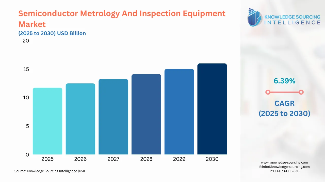
The semiconductor metrology and inspection equipment market, with a 6.39% CAGR, is set to grow to USD 15.987 billion by 2030 from USD 11.728 billion in 2025.
Highlights:
- 1Increasing semiconductor demandis driving growth in the metrology and inspection equipment market.
- 2Growing AI and 5G adoptionis boosting the need for advanced inspection tools.
- 3Asia Pacificis leading the metrology equipment market with robust manufacturing.
- 4Advancing lithography technologiesare enhancing precision in semiconductor quality control.
- 5Rising electronics productionis fueling demand for wafer inspection systems.
- 6Expanding government investmentsare supporting metrology and inspection equipment growth.
- 7Strengthening quality control focusis promoting the use of advanced metrology solutions.
Semiconductor metrology and inspection equipment are specialized tools used in the semiconductor industry to measure and monitor various parameters related to the manufacturing process. These tools are critical to ensuring the quality and reliability of semiconductor products. The semiconductor metrology and inspection equipment market is driven by a combination of increasing demand for semiconductor devices, technological advancements, regulations and standards, the increasing complexity of semiconductor devices, and a growing focus on quality control.
Semiconductor Metrology and Inspection Equipment Market Driver:
- Increasing investments in the development of the semiconductor industry are anticipated to boost the market growth of semiconductor metrology and inspection equipment.
Growing in significance and usage across multiple applications, including electronics, automotive, healthcare, and telecommunications, the semiconductor industry is seeing increasing investments from both companies and governments worldwide. The rise in investments is expected to drive demand for semiconductor metrology and inspection equipment. For instance, Intel Corporation, the leading manufacturer of semiconductor chips globally, announced its commitment to invest a minimum of $20 billion in two novel factories aimed at producing semiconductors in September 2022. Micron Technology marked the inauguration of a new manufacturing site near Syracuse, N.Y., in October 2022, with plans to invest around $20 billion in the facility. Taiwan Semiconductor Manufacturing Company (TSMC) announced its plans to triple its investment to $40 billion and construct a second advanced chip factory in Phoenix, Arizona, in December 2022. In September 2021, Economy Minister Peter Altmaier engaged in discussions with 50 representatives from the semiconductor industry at both European and international levels to encourage investment in microelectronics in Germany.
Additionally, the German government revealed plans to invest approximately €3 billion towards the redevelopment of production sites throughout the semiconductor production value chain. The Italian government declared its intentions in March 2022 to allocate over 4 billion euros ($4.6 billion) towards increasing local chip manufacturing until 2030. France announced an investment plan worth €5 billion in July 2022 with the goal of developing and manufacturing advanced electronics technology by 2030. Thus, the market expansion of semiconductor metrology and inspection equipment will be propelled by investments from countries worldwide.
Semiconductor Metrology and Inspection Equipment Market Geographical Outlook:
- The Asia-Pacific region is expected to show the maximum growth potential for the semiconductor metrology and inspection equipment market.
The growth of this market can be attributed to the significant presence of semiconductor manufacturing industries in countries such as China, Japan, South Korea, and Taiwan. For instance, according to data published by the National Bureau of Statistics (NBS), the production of integrated circuits (ICs) in China during January and February 2023 reached a total of 44.3 billion units. Japan’s semiconductor industry experienced a 26.2% growth in 2021, according to the International Trade Administration. According to the Industrial Technology Research Institute (ITRI), the semiconductor industry in Taiwan achieved a total production value of NT$4.08 trillion (equivalent to US$146.76 billion) in 2021, indicating a 26.7% increase year-on-year.
Additionally, the region has a large consumer electronics market and increasing investments in semiconductor research and development, which are expected to drive the demand for semiconductor metrology and inspection equipment. For instance, data from the Ministry of Electronics and Information Technology states that India’s electronics manufacturing industry was valued at US$74.7 billion in 2020. According to the same source, India can achieve over US$300 billion in electronics manufacturing and exports by 2025. Similarly, data from Japan’s Ministry of Economy, Trade and Industry indicates that in 2020, the country produced around 29,362 million yen worth of consumer electronic equipment.
Moreover, in September 2022, as part of the PLI (production-linked incentive) scheme, a budget of Rs 76,000 crore (approximately $10 billion) was allocated for the creation of a semiconductor and display manufacturing electronics ecosystem in India. In November 2022, The Japanese government declared its plans to allocate an initial investment of 70 billion yen (equivalent to $500 million) towards a novel semiconductor venture, which will be spearheaded by technology companies such as Sony Group Corp and NEC Corp. Thus, the combination of such factors is expected to boost the market growth of semiconductor metrology and inspection equipment in the Asia Pacific region.
Semiconductor Metrology and Inspection Equipment Market Key Developments:
- October 2025: Applied Materials introduced the PROVision™ 10 eBeam Metrology System, providing sub-nanometer resolution metrology crucial for controlling the yield of complex 3D chips and advanced logic structures.
- October 2025: Lasertec released the ACTIS A200HiT actinic EUV patterned mask inspection system, offering triple the speed of its predecessor for detecting printable defects in wafer fabs.
- October 2025: Nordson Test & Inspection announced a broad suite of next-gen inspection/metrology equipment, including Multi-Function AOI/SPI/CMM systems, automated X-ray (AXI), and acoustic micro-imaging (AMI), aimed at advanced packaging, SMT, and wafer-level inspection.
- February 2025: TASMIT Inc. launched the INSPECTRA inspection system, the industry's first to inspect large glass substrates for backside/internal defects, critical for advanced packaging quality control.
List of Top Semiconductor Metrology and Inspection Equipment Companies:
- KLA Corporation
- Applied Materials Inc
- Onto Innovation Inc
- Thermo Fisher Scientific Inc
- Hitachi Hi-Technologies Corporation
Semiconductor Metrology and Inspection Equipment Market Scope:
| Report Metric | Details |
|---|---|
| Study Period | 2021 to 2031 |
| Historical Data | 2021 to 2024 |
| Base Year | 2025 |
| Forecast Period | 2026 – 2031 |
| Report Metric | Details |
| Semiconductor Metrology and Inspection Equipment Market Size in 2025 | USD 11.728 billion |
| Semiconductor Metrology and Inspection Equipment Market Size in 2030 | USD 15.987 billion |
| Growth Rate | CAGR of 6.39% |
| Study Period | 2020 to 2030 |
| Historical Data | 2020 to 2023 |
| Base Year | 2024 |
| Forecast Period | 2025 – 2030 |
| Forecast Unit (Value) | USD Billion |
| Segmentation |
|
| Geographical Segmentation | North America, South America, Europe, Middle East and Africa, Asia Pacific |
| List of Major Companies in Semiconductor Metrology and Inspection Equipment Market |
|
| Customization Scope | Free report customization with purchase |
Semiconductor Metrology and Inspection Equipment Market Segmentation:
- SEMICONDUCTOR METROLOGY AND INSPECTION EQUIPMENT MARKET BY TYPE
- Lithography Metrology
- Thin Film Metrology
- Wafer Inspection
- Lead Frame Inspection
- Others
- SEMICONDUCTOR METROLOGY AND INSPECTION MARKET BY TECHNOLOGY
- Optical
- E-beam
- SEMICONDUCTOR METROLOGY AND INSPECTION MARKET BY GEOGRAPHY
- North America
- USA
- Canada
- Mexico
- South America
- Brazil
- Argentina
- Others
- Europe
- Germany
- France
- United Kingdom
- Spain
- Others
- Middle East and Africa
- Saudi Arabia
- UAE
- Others
- Asia Pacific
- China
- India
- Japan
- South Korea
- Indonesia
- Thailand
- Others
- North America
Market Segmentation
By Type
By Technology
By Geography
Table of Contents
1. EXECUTIVE SUMMARY
2. MARKET SNAPSHOT
2.1. Market Overview
2.2. Market Definition
2.3. Scope of the Study
2.4. Market Segmentation
3. BUSINESS LANDSCAPE
3.1. Market Drivers
3.2. Market Restraints
3.3. Market Opportunities
3.4. Porter’s Five Forces Analysis
3.5. Industry Value Chain Analysis
3.6. Policies and Regulations
3.7. Strategic Recommendations
4. TECHNOLOGICAL OUTLOOK
5. SEMICONDUCTOR METROLOGY AND INSPECTION EQUIPMENT MARKET BY TYPE
5.1. Introduction
5.2. Lithography Metrology
5.3. Thin Film Metrology
5.4. Wafer Inspection
5.5. Lead Frame Inspection
5.6. Others
6. SEMICONDUCTOR METROLOGY AND INSPECTION MARKET BY TECHNOLOGY
6.1. Introduction
6.2. Optical
6.3. E-beam
7. SEMICONDUCTOR METROLOGY AND INSPECTION MARKET BY GEOGRAPHY
7.1. Introduction
7.2. North America
7.2.1. USA
7.2.2. Canada
7.2.3. Mexico
7.3. South America
7.3.1. Brazil
7.3.2. Argentina
7.3.3. Others
7.4. Europe
7.4.1. Germany
7.4.2. France
7.4.3. United Kingdom
7.4.4. Spain
7.4.5. Others
7.5. Middle East and Africa
7.5.1. Saudi Arabia
7.5.2. UAE
7.5.3. Others
7.6. Asia Pacific
7.6.1. China
7.6.2. India
7.6.3. Japan
7.6.4. South Korea
7.6.5. Indonesia
7.6.6. Thailand
7.6.7. Others
8. COMPETITIVE ENVIRONMENT AND ANALYSIS
8.1. Major Players and Strategy Analysis
8.2. Market Share Analysis
8.3. Mergers, Acquisitions, Agreements, and Collaborations
8.4. Competitive Dashboard
9. COMPANY PROFILES
9.1. KLA Corporation
9.2. Applied Materials Inc
9.3. Onto Innovation Inc
9.4. Thermo Fisher Scientific Inc
9.5. Hitachi High-Technologies Corporation
9.6. Nova Measuring Instruments Limited
9.7. ASML Holding NV
9.8. Lasertec Corporation
9.9. Nikon Precision Inc
9.10. Canon
10. APPENDIX
10.1. Currency
10.2. Assumptions
10.3. Base and Forecast Years Timeline
10.4. Key benefits for the stakeholders
10.5. Research Methodology
10.6. Abbreviations
LIST OF FIGURES
LIST OF TABLES
Navigate
Trusted by the world's leading organizations


