Report Overview
Semiconductor Packaging Material Market Size:
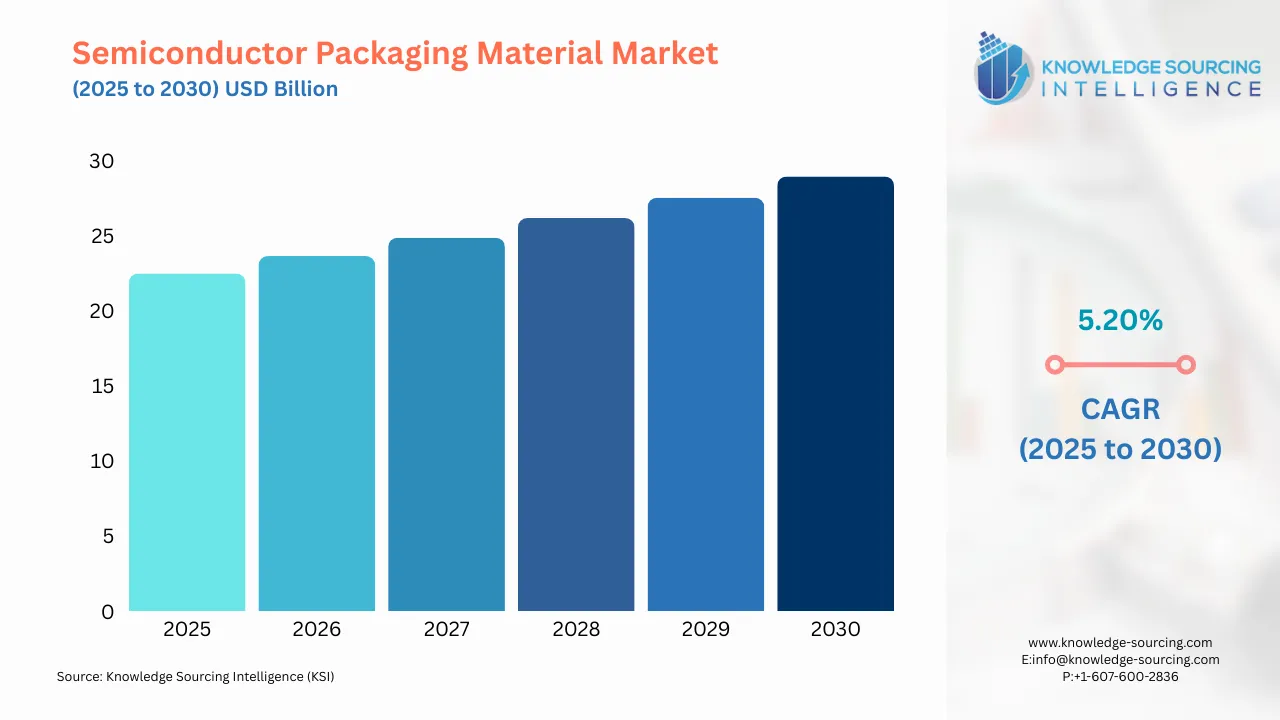
The semiconductor packaging material market is expected to grow from USD 22.476 billion in 2025 to USD 28.953 billion in 2030, at a CAGR of 5.20%.
Highlights:
- 1Increasing automation adoptionis driving demand for semiconductor packaging materials.
- 2Growing electronics marketis boosting the need for reliable chip packaging solutions.
- 3Asia Pacificis leading the semiconductor packaging material market with industrial growth.
- 4Advancing IoT and AI technologiesare fueling demand for advanced packaging materials.
- 5Rising electric vehicle productionis enhancing the need for durable semiconductor packaging.
- 6Expanding consumer gadget demandis promoting growth in packaging material usage.
- 7Strengthening industrial investmentsare supporting the semiconductor packaging material market expansion.
The Semiconductor Packaging is used to protect the ICs and semiconductors from corrosion and other environmental conditions and therefore ensures a stable connection of the chip. These semiconductor chips are therefore used in various industrial segments, including automotive, aerospace, electronics, manufacturing, healthcare, etc., and constitute an important material used in the production process.
Semiconductor Packaging Material Market Trends:
Semiconductor Packaging Material Industry is directly related to the semiconductor industry of the globe. The rapid Industrialization, powered by a high scale of investment in manufacturing, automotive, and other sectors, is the major driving factor behind the growth of the Semiconductor Packaging Material Market. Growing penetration of IoT, Machine Learning, etc., is expected to play an integral role in the development of the semiconductor packaging material market. Also, the growing demand for electronic gadgets is directly proportional to the semiconductor market growth, therefore positively impacting the Semiconductor Packaging Material Market. Asia-Pacific is expected to have the highest market share in the market in this market owing to the presence of key industries in this region. Besides that, the low cost of labor, increasing demand for electronic gadgets, and technological advancement in the region are expected to play a vital role in the market development.
The global shortage of semiconductor chips is one of the major restraints that is projected to hamper market growth in the coming years. Besides that, high labor costs and increasing cost of raw materials can also serve as severe obstacles to the market growth.
Semiconductor Packaging Material Market Factors:
- Increasing Automation and Industrial Investment:
The rising industrial investment in the economies around the globe, powered by high-scale adoption of IoT, automation, technical advancement, Artificial Intelligence, Cloud-based Software, etc., is expected to contribute significantly towards the Semiconductor Packaging Material market. This is because a semiconductor chip is a vital tool that is always in high demand across various industries like automotive, aerospace, electronics, etc. High industrial growth is therefore linked with high demand for semiconductor chips, and to ensure their durability and performance, the packaging material market can experience vital growth.
One of the prime examples of that is the increasing Robot Density (the proportion of the total number of operational robots in industries relative to the number of industrial workers) around the globe, which is used to track the automation adoption in a region. Robots require semiconductors in their processing units to gather external information and data. According to the International Federation of Robotics, average robot density in the manufacturing industry hit a new global record of 126 units per 10,000 employees. With the rising technological advancement, these statistics hold a positive future for the semiconductor packaging material market due to its wide-scale adoption in robot manufacturing and handling.
- Increasing adoption of Electronic Gadgets:
The economic development of the nations has positively impacted the disposable income of the people. This has significantly contributed towards the change in living standards and has positively impacted the electronic gadgets market by the rising adoption of smartphones, laptops, etc. Electronic companies use semiconductor chips in high numbers, and with the projected increase in their adoption in the coming years, the need for semiconductor material packaging is also expected to witness significant growth.
One of the prime examples under this is the increasing use of electric and hybrid vehicles, which is a significant highlight for this market. Electric Vehicles are the future of the globe, and their vehicle battery and software systems require semiconductors to access various functions. This requires corrosion-free and undamaged semiconductors, which are provided by its packaging and material market. Therefore, with the growing adoption of EVs, the semiconductor chips packaging material market stands in a significant position.
Semiconductor Packaging Material Market Restraints:
- Shortage of Semiconductor Chips:
Currently, the world is going through a major problem of semiconductor shortage. The pandemic has put enormous pressure on this industry with the imbalance between high demand and low supply. This has severely impacted the electronics and automation industries. With the fall in the production of semiconductor chips, the semiconductor material packaging market also took a hit. The production of the chips has still not revived, and this holds the possibility for major restraints for the Semiconductor Packaging Material Market.
- The increasing cost of Raw Materials:
Another major restraint for the Semiconductor Packaging Material Market is the high cost of raw materials. Several factors, like the increasing price of copper, shipping charges, and shortage of semiconductors, are responsible for this surge in cost, which can hold various restraints for the growth of the semiconductor packaging Material Market.
Semiconductor Packaging Material Market Key Developments:
- November 2025: Samsung Electro-Mechanics and Sumitomo Chemical formed a joint venture to produce Glass Core, a next-gen substrate for AI and HPC packaging.
- September 2025: LG Chem developed a proprietary liquid Photo-Imageable Dielectric (PID) for advanced semiconductor packaging, targeting high-performance AI and HPC markets.
- September 2025: LCY Chemical Corp. launched advanced polymer and CPI formulations for high-density semiconductor packaging, enabling reliable AI, high-speed communications, and next-generation display applications.
- March 2025: DuPont introduced Circuposit™ SAP8000 metallization and advanced interconnect materials optimized for IC substrates, supporting AI/server-class chip packaging applications.
List of Top Semiconductor Packaging Material Companies:
- Dow Inc.
- Henkel AG & Co. KGaA
- Sumitomo Chemical Co., Ltd.
- BASF SE
- Hitachi Chemical Co., Ltd.
Semiconductor Packaging Material Market Scope:
| Report Metric | Details |
|---|---|
| Study Period | 2021 to 2031 |
| Historical Data | 2021 to 2024 |
| Base Year | 2025 |
| Forecast Period | 2026 – 2031 |
| Report Metric | Details |
| Semiconductor Packaging Material Market Size in 2025 | USD 22.476 billion |
| Semiconductor Packaging Material Market Size in 2030 | USD 28.953 billion |
| Growth Rate | CAGR of 5.20% |
| Study Period | 2020 to 2030 |
| Historical Data | 2020 to 2023 |
| Base Year | 2024 |
| Forecast Period | 2025 – 2030 |
| Forecast Unit (Value) | USD Billion |
| Segmentation |
|
| Geographical Segmentation | North America, South America, Europe, Middle East and Africa, Asia Pacific |
| List of Major Companies in Semiconductor Packaging Material Market |
|
| Customization Scope | Free report customization with purchase |
Semiconductor Packaging Material Market Segmentation:
- By Type
- Organic Substrates
- Bonding Wires
- Lead-frames
- Ceramic Package
- Die Attach Material
- Others
- By Industry Vertical
- Consumer Electronics
- Automotive
- Healthcare
- IT & Telecommunication
- Aerospace and Defense
- Others
- By Technology
- Grid Array
- Small Outline Package
- Quad Flat Package
- Dual-flat no-leads
- Single In-Line Package
- Dual In-Line Package
- Others
- By Geography
- North America
- USA
- Canada
- México
- South America
- Brazil
- Argentina
- Others
- Europe
- U.K.
- Germany
- France
- Others
- Middle East and Africa
- UAE
- South Africa
- Israel
- Saudi Arabia
- Others
- Asia-Pacific
- China
- Japan
- India
- Australia
- Taiwan
- South Korea
- Others
- North America
Our Best-Performing Industry Reports:
Table of Contents
1. INTRODUCTION
1.1. Market Definition
1.2. Market Segmentation
2. RESEARCH METHODOLOGY
2.1. Research Data
2.2. Assumptions
3. EXECUTIVE SUMMARY
3.1. Research Highlights
4. MARKET DYNAMICS
4.1. Market Drivers
4.2. Market Restraints
4.3. Porters Five Forces Analysis
4.3.1. Bargaining Power of Suppliers
4.3.2. Bargaining Power of Buyers
4.3.3. The Threat of New Entrants
4.3.4. Threat of Substitutes
4.3.5. Competitive Rivalry in the Industry
4.4. Industry Value Chain Analysis
5. SEMICONDUCTOR PACKAGING MATERIAL MARKET ANALYSIS, BY TYPE
5.1. Introduction
5.2. Organic Substrates
5.3. Bonding Wires
5.4. Lead-frames
5.5. Ceramic Package
5.6. Die Attach Material
5.7. Others
6. SEMICONDUCTOR PACKAGING MATERIAL MARKET ANALYSIS, BY INDUSTRY VERTICAL
6.1. Introduction
6.2. Consumer Electronics
6.3. Automotive
6.4. Healthcare
6.5. IT & Telecommunication
6.6. Aerospace and Defense
6.7. Others
7. SEMICONDUCTOR PACKAGING MATERIAL MARKET ANALYSIS, BY TECHNOLOGY
7.1. Introduction
7.2. Grid Array
7.3. Small Outline Package
7.4. Quad Flat Package
7.5. Dual-flat no-leads
7.6. Single In-Line Package
7.7. Dual In-Line Package
7.8. Others
8. SEMICONDUCTOR PACKAGING MATERIAL MARKET ANALYSIS, BY GEOGRAPHY
8.1. Introduction
8.2. North America
8.2.1. USA
8.2.2. Canada
8.2.3. Mexico
8.3. South America
8.3.1. Brazil
8.3.2. Argentina
8.3.3. Others
8.4. Europe
8.4.1. U.K.
8.4.2. Germany
8.4.3. France
8.4.4. Others
8.5. Middle East and Africa
8.5.1. UAE
8.5.2. South Africa
8.5.3. Israel
8.5.4. Saudi Arabia
8.5.5. Others
8.6. Asia Pacific
8.6.1. China
8.6.2. Japan
8.6.3. India
8.6.4. Australia
8.6.5. Taiwan
8.6.6. South Korea
8.6.7. Others
9. COMPETITIVE ENVIRONMENT AND ANALYSIS
9.1. Major Players and Strategy Analysis
9.2. Emerging Players and Market Lucrativeness
9.3. Mergers, Acquisitions, Agreements, and Collaborations
9.4. Vendor Competitiveness Matrix
10. COMPANY PROFILES 10.1. Dow Inc. 10.2. Henkel AG & Co. KGaA 10.3. Sumitomo Chemical Co., Ltd. 10.4. BASF SE 10.5. Hitachi Chemical Co., Ltd. 10.6. DuPont de Nemours, Inc. 10.7. Samsung Electro-Mechanics Co., Ltd. 10.8. Shin-Etsu Chemical Co., Ltd. 10.9. LG Chem Ltd. 10.10. Jiangsu ChangJian Technology Co., Ltd.
Navigate
Trusted by the world's leading organizations


