Report Overview
Electronic Design Automation Market Size & Forecast:
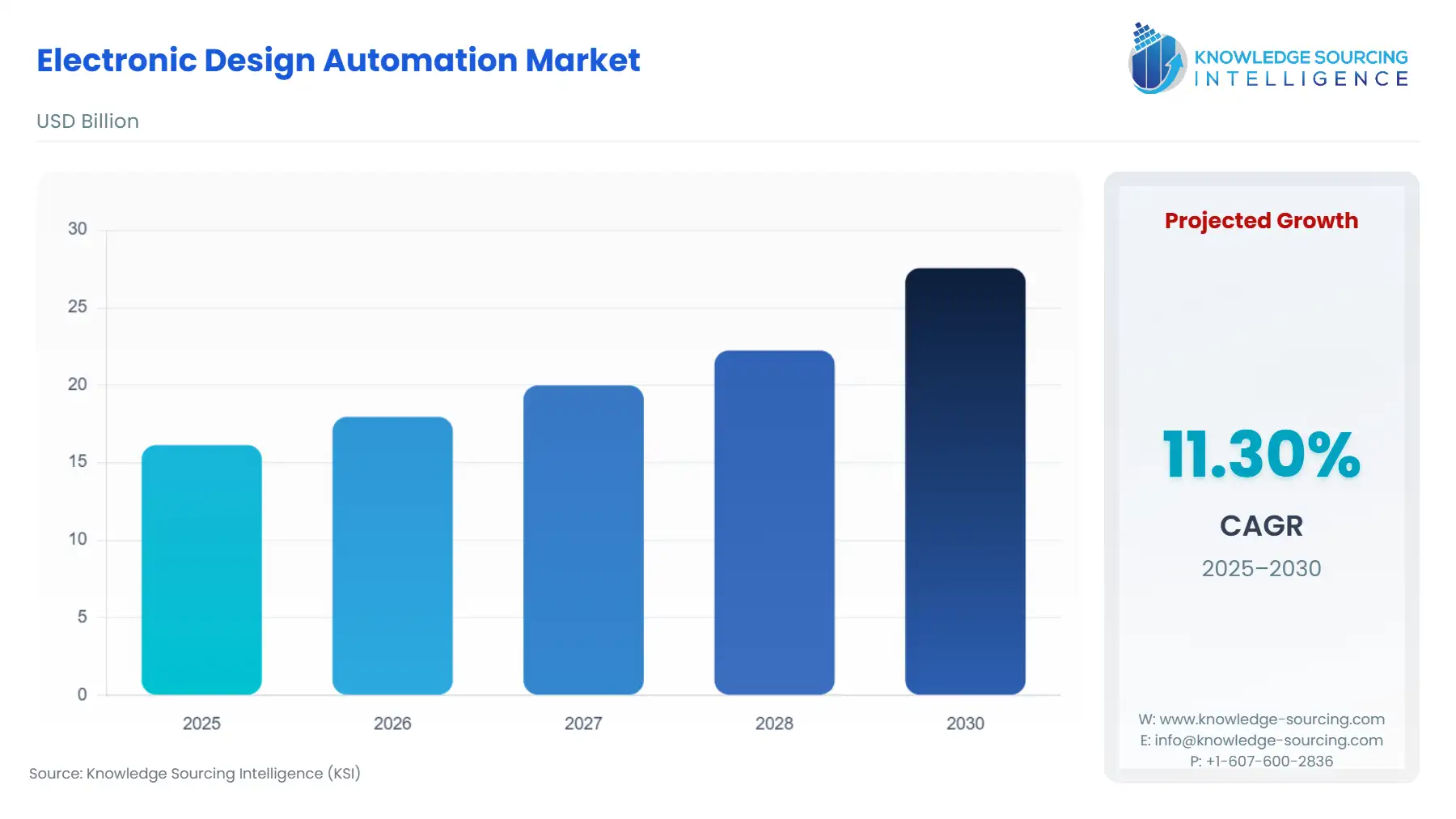
Electronic Design Automation Market, at a 11.30% CAGR, is anticipated to achieve USD 27.551 billion by 2030 from USD 16.134 billion in 2025.
Highlights:
- 1The shift to advanced semiconductor architectures, specifically the rise of chiplets and 2.5D/3D heterogeneous integration, creates an urgent, direct demand for sophisticated Electronic Design Automation (EDA) tools capable of multi-die system-level analysis, a critical factor propelling the Computer-Aided Engineering (CAE) segment.
- 2Geopolitical tensions have introduced significant volatility, exemplified by the brief but disruptive imposition and subsequent reversal of US export controls on EDA software to China in 2025, which immediately impacted Chinese design teams and accelerated calls for domestic EDA alternatives.
- 3The escalating complexity in automotive electronics, driven by Advanced Driver Assistance Systems (ADAS) and autonomous vehicle development, necessitates integrated electronic and multiphysics simulation, directly increasing demand for specialized EDA solutions that cover structures, fluids, and electromagnetics.
- 4Major market consolidation continues, with top players leveraging strategic acquisitions to bridge the gap between silicon-level design and system-level physics, as demonstrated by Synopsys' completion of the Ansys acquisition in July 2025.
The Electronic Design Automation (EDA) market provides the critical software, hardware, and intellectual property that forms the foundation of modern semiconductor design and verification. This ecosystem of tools is the non-negotiable prerequisite for developing the complex Integrated Circuits (ICs) and systems central to global technological progress. The current market dynamic is defined by an unprecedented convergence of foundational technology shifts and volatile macroeconomic forces. The transition to advanced silicon nodes, coupled with the systemic integration of artificial intelligence (AI) and machine learning (ML) into design flows, mandates a fundamental evolution in EDA capability, moving from siloed chip-level design to a holistic "silicon-to-systems" approach. This imperative for integrated, highly automated design is directly translating into sustained, high-value demand for advanced EDA licenses and platforms.
________________________________________
Electronic Design Automation Market Growth Drivers:
The move toward heterogeneous computing and chiplet architecture is the foremost catalyst for advanced EDA demand. Traditional monolithic chip design faces physical and economic scaling constraints at sub-5nm nodes. Chiplets resolve this by allowing complex systems to be fabricated as an assemblage of specialized dies (chiplets) interconnected on an interposer. This architecture creates a critical and immediate need for novel EDA solutions that address inter-die communication, power integrity, and thermal management across the entire package. Specifically, this environment propels demand for sophisticated 2.5D/3D IC Physical Design & Verification tools and CAE software for multi-physics simulation, as these solutions are essential for modeling the high-bandwidth, low-latency communication that defines chiplet-based performance.
The integration of Artificial Intelligence (AI) and Machine Learning (ML) into EDA workflows directly increases demand for automated and generative design tools. As chip complexity outstrips human capacity for manual optimization, AI-driven EDA solutions, such as those for generative IC design and multi-run verification, become indispensable for maintaining design quality and reducing cycle time. This shift is not a generic sector trend but a specific demand driver for advanced software licenses that can leverage massive compute resources for autonomous design space exploration, translating directly into higher subscription revenues for AI-enabled EDA platforms.
- Challenges and Opportunities
The primary challenge constraining market growth is the persistent security and data sovereignty concern surrounding Cloud-Based EDA deployment. While the scalability and cost-efficiency of the cloud offer a clear opportunity especially for compute-intensive verification tasks—many semiconductor firms remain hesitant to migrate proprietary, mission-critical silicon designs and Intellectual Property (IP) off-premise. This perception of reduced security, particularly regarding data breaches and unauthorized access in a multi-tenant environment, directly suppresses the demand for 'Cloud-Based' deployment models, forcing a continued reliance on high-capital 'On-Premise' licenses and infrastructure. Conversely, this constraint presents an opportunity for EDA vendors to invest in highly secure, hybrid cloud architectures that provide verifiable encryption and access control, thereby unlocking pent-up demand.
A secondary challenge is the escalating scarcity of highly specialized EDA engineering talent required to operate and optimize advanced tools. The sophistication of next-generation tools, particularly in areas like quantum computing and advanced node physical design, creates a skills gap. This increases the total cost of ownership for EDA solutions, as companies must invest heavily in training or risk inefficient tool utilization. This challenge, however, generates a parallel opportunity: a higher demand for turnkey, System Design and Analysis tools and professional services from EDA vendors, which can partially compensate for the internal talent deficit.
- Raw Material and Pricing Analysis
Electronic Design Automation (EDA) is fundamentally a software and Intellectual Property (IP) service, not a physical product. As such, it does not have a conventional 'raw material' supply chain based on chemicals, metals, or physical components. The core 'inputs' are human capital (highly skilled software engineers) and compute infrastructure (servers and cloud credits). Consequently, this market analysis omits a traditional raw material and pricing section. Pricing dynamics are tied to licensing models (perpetual versus subscription), the computational intensity of the design process (e.g., hardware-assisted verification platform costs), and the value of the embedded IP, rather than commodity pricing fluctuations.
- Supply Chain Analysis
The EDA supply chain is highly concentrated and knowledge-intensive. At its core, it is a design-centric dependency where global semiconductor manufacturing (fabs and foundries) is dependent on a highly consolidated group of EDA providers. The supply chain moves from EDA software firms (IP/Tools), Integrated Device Manufacturers (IDMs) and Fabless Design Houses, Wafer Fabs/Foundries, Assembly, Test, and Packaging, Electronics Original Equipment Manufacturers (OEMs). The key dependencies are technical interoperability; the tools must be certified for the latest manufacturing processes (e.g., TSMC's N3/N2 nodes) before a chip can be successfully taped out. Any disruption in EDA tool access or development immediately halts the front end of the entire global semiconductor supply chain, as demonstrated by recent geopolitical restrictions. The primary production hubs remain in North America and Asia-Pacific due to the proximity of major R&D centers and leading foundries.
Electronic Design Automation Market Government Regulations:
|
Jurisdiction |
Key Regulation / Agency |
Market Impact Analysis |
|
United States |
Export Administration Regulations (EAR) / Bureau of Industry and Security (BIS) |
High Demand Volatility & Strategic Re-Alignment. Restrictions targeting advanced-node design tools (e.g., GAAFET-specific EDA) immediately suspend licenses to certain foreign entities, creating significant, albeit temporary, revenue losses for US-based EDA firms. This action concurrently acts as a catalyst for affected jurisdictions to aggressively fund and promote domestic EDA alternatives, strategically shifting long-term global demand towards new players. |
|
European Union |
EU AI Act (Proposed) / European Commission |
Compliance-Driven Design Imperative. While not directly regulating EDA tools, the Act's focus on transparency, safety, and non-discrimination for high-risk AI applications (many of which are executed on custom silicon) creates an indirect demand for EDA tools that provide verifiable, auditable design flows for chip design, enhancing the demand for advanced verification and functional safety features. |
|
India |
Design Linked Incentive (DLI) Scheme / India Semiconductor Mission (ISM) |
Direct Stimulus for New Demand. The DLI scheme explicitly promotes and funds domestic semiconductor design startups by providing financial support and granting access to state-of-the-art EDA tools and foundry services. This governmental intervention creates a direct, subsidized demand channel for EDA software licenses among emerging local design houses. |
Electronic Design Automation Market Segment Analysis:
- By Technology: Semiconductor Intellectual Property (SIP)
The Semiconductor Intellectual Property (SIP) segment, which includes pre-designed, reusable blocks like processor cores, interface IPs (e.g., SerDes), and memory controllers, is a critical enabler for the design ecosystem. SIP's demand is accelerating because it addresses the principal industry constraint: design complexity versus time-to-market. As chip designs incorporate billions of transistors and are required to support hyper-complex functions (e.g., 5G, AI inference), companies cannot afford to design every component from scratch. The reuse of pre-verified, hardened IP blocks substantially reduces design risk, cuts verification time, and shortens product development cycles. This necessity drives immediate commercial demand for SIP licenses and associated royalty streams, making SIP a high-growth segment. The rising adoption of advanced processor IP—expected to hold the largest share by 2025—is particularly pronounced, driven by the need for customized, high-performance computing in data centers and autonomous systems. This market dynamic explicitly mandates the procurement of third-party SIP to remain competitive, directly bolstering SIP revenue growth.
- By Application: Automotive
The Automotive sector is undergoing a profound transformation that directly converts new design requirements into demand for EDA. The shift from mechanically-driven systems to Software-Defined Vehicles (SDVs), coupled with the development of Advanced Driver Assistance Systems (ADAS) and autonomous platforms, mandates an unprecedented integration of electronic components. These systems are characterized by extremely stringent functional safety requirements (e.g., ISO 26262) and highly complex sensor data fusion, requiring custom System-on-Chips (SoCs). This demands EDA tools that not only perform conventional silicon design but also offer specialized capabilities for mixed-signal design, robust multiphysics simulation (to model the effects of temperature, vibration, and electromagnetic interference on the chip and package), and comprehensive functional safety verification. The automotive design cycle, being long and safety-critical, mandates high-fidelity verification platforms, which directly stimulates demand for high-value CAE and verification software suites to ensure the silicon's integrity under real-world vehicle operation.
________________________________________
Electronic Design Automation Market Geographical Analysis
- US Market Analysis (North America)
The US market remains the global EDA epicenter, driven by the presence of both the world's leading EDA vendors and the largest fabless design houses (e.g., NVIDIA, AMD). Local demand is propelled by colossal investments in AI and hyperscale data center infrastructure, which necessitate the continuous design of custom, cutting-edge AI accelerators and high-performance CPUs. Furthermore, substantial government R&D and defense spending act as a strong anchor for demand, particularly for advanced verification and system-level modeling tools to ensure supply chain security and performance superiority. The focus is on the most advanced technology nodes and the early commercialization of new architectures like chiplets.
- Brazil Market Analysis (South America)
The Brazilian EDA market is in an emergent phase, with demand primarily centered on the Consumer Electronics and Telecommunications sectors, albeit focused on more mature process nodes compared to the US. Local demand is characterized by a need for cost-effective PCB and multi-chip module (MCM) tools to support domestic electronics assembly and manufacturing. The primary constraint is a smaller local fab infrastructure, which limits advanced IC design activity. However, government-supported initiatives aimed at fostering local semiconductor design talent and integrating into global value chains could create future, targeted demand for entry-level and educational EDA licenses.
- Germany Market Analysis (Europe)
Germany's demand for EDA is overwhelmingly concentrated in the high-value Automotive and Industrial sectors, reflecting the country's manufacturing strengths. Local demand is defined by the imperative for functional safety (ISO 26262 compliance) in automotive electronics and robust, highly reliable chips for Industry 4.0 applications. This mandates a high uptake of sophisticated verification, safety-critical IP, and integrated multiphysics simulation tools. The strict quality and regulatory environment in Europe creates a specific, non-negotiable demand for EDA solutions that can prove design robustness and compliance across the entire electronic system.
- Saudi Arabia Market Analysis (Middle East & Africa)
EDA demand in Saudi Arabia is largely nascent but is emerging under the umbrella of national diversification and technology initiatives like Vision 2030. Current demand is predominantly driven by public-sector investment in defense and strategic technology projects, alongside growing telecommunications and hyperscale data center construction. Local factors focus demand on procuring high-end design services and training to rapidly establish domestic semiconductor design capabilities. The market sees less organic, commercial demand from established fabless companies but a strong strategic demand fueled by national development funds, often preferring flexible, cloud-based deployment models for rapid scaling.
- India Market Analysis (Asia-Pacific)
The Indian EDA market is experiencing aggressive growth, fueled by both the India Semiconductor Mission (ISM) and its Design Linked Incentive (DLI) scheme. This government support directly subsidizes the establishment of new semiconductor design startups and MSMEs, creating a surge in demand for EDA tools, foundry access, and design IP support. India has a significant concentration of global R&D and design centers, driving demand for all categories of EDA, particularly in the SIP and CAE segments. The local market is a key growth area for both leading global vendors and emerging domestic EDA firms, making it a highly dynamic region where policy directly translates to commercial opportunity.
________________________________________
Electronic Design Automation Market Competitive Analysis:
The Electronic Design Automation market is an effective oligopoly, highly concentrated around three dominant, full-stack vendors: Synopsys, Cadence Design Systems, and Siemens (through its Mentor Graphics acquisition). Competition centers on the capability to deliver a unified, certified flow across the most advanced process nodes and to expand the portfolio to address system-level design challenges beyond the chip (e.g., packaging, thermal, and structural analysis). The primary competitive axis has shifted to integrating AI/ML capabilities for design autonomy and strategic acquisitions that extend the vendors' total addressable market (TAM).
Cadence Design Systems Cadence strategically positions itself around its Intelligent System Design™ strategy, focusing on delivering end-to-end solutions from IP to system verification. A core strength is its portfolio covering advanced node digital and signoff tools, complemented by strong analog/mixed-signal capabilities. The company’s focus on the convergence of electronics and mechanical design is evident in its key strategic moves. For instance, the agreement to acquire Hexagon's Design & Engineering business in September 2025 (expected to close Q1 2026) is aimed at integrating Hexagon’s multiphysics simulation software, which includes industry-standard tools like MSC Nastran and Adams, used in aerospace and automotive sectors. This action directly expands Cadence's reach into the multi-billion-dollar structural analysis market, bolstering its System Design and Analysis revenue stream and addressing the imperative for system-level verification.
Synopsys Synopsys maintains its market leadership through a comprehensive portfolio spanning core EDA, extensive Semiconductor Intellectual Property (SIP) offerings, and system-level verification solutions. Its strategy is anchored by its AI-driven Synopsys.ai™ platform, which embeds generative AI and ML across the full design flow, from specification to tapeout. A pivotal, transformative move was the completion of its acquisition of Ansys in July 2025. This merger integrates Ansys' world-class simulation and analysis capabilities including its physics-based tools for electromagnetics, fluids, and structures into Synopsys' core silicon design platform. This acquisition is explicitly designed to accelerate the 'Silicon to Systems' approach, enabling customers to simulate the performance of their chips within their larger electronic systems (e.g., in an autonomous vehicle or a server rack), significantly expanding Synopsys' TAM and fortifying its competitive position in the high-growth automotive and aerospace segments.
________________________________________
Electronic Design Automation Market Developments:
- September 2025: Cadence Design Systems, Inc. agreed to acquire the Design & Engineering (D&E) business of Hexagon AB for approximately €2.7 billion. The D&E business includes core multiphysics simulation software such as MSC Nastran and Adams. This acquisition directly supports Cadence’s Intelligent System Design strategy by significantly expanding its multiphysics system analysis portfolio, which is essential for the design and validation of complex mechanical and converged systems. The transaction is expected to close in the first quarter of 2026.
- July 2025: Synopsys, Inc. completed its acquisition of Ansys, Inc. The merger was presented as the creation of a leader in 'silicon to systems' design solutions, combining Synopsys' expertise in semiconductor design technology and IP with Ansys' simulation and analysis capabilities. This strategic move is expected to accelerate the development of integrated electronic and physics-based design solutions, directly enhancing Synopsys’ offerings in high-growth adjacent markets like automotive and aerospace.
________________________________________
Electronic Design Automation Market Scope:
| Report Metric | Details |
|---|---|
| Total Market Size in 2026 | USD 16.134 billion |
| Total Market Size in 2031 | USD 27.551 billion |
| Growth Rate | 11.30% |
| Study Period | 2021 to 2031 |
| Historical Data | 2021 to 2024 |
| Base Year | 2025 |
| Forecast Period | 2026 – 2031 |
| Segmentation | Type, Deployment, Application, Geography |
| Geographical Segmentation | North America, South America, Europe, Middle East and Africa, Asia Pacific |
| Companies |
|
Electronic Design Automation Market Segmentation:
- By Type
- Computer-Aided Engineering (CAE)
- IC Physical Design & Verification
- Printed Circuit Board (PCB) and Multi-Chip Module (MCM)
- Semiconductor Intellectual Property (SIP)
- Others
- By Deployment
- On-Premise
- Cloud-Based
- By Application
- Aerospace & Defence
- Automotive
- Consumer Electronics
- Industrial
- Medical
- Telecommunications
- By Geography
- North America (USA, Canada, Mexico)
- South America (Brazil, Argentina, Others)
- Europe (Germany, France, United Kingdom, Spain, Others)
- Middle East and Africa (Saudi Arabia, UAE, Others)
- Asia Pacific (China, India, Japan, South Korea, Indonesia, Thailand, Others)
Our Best-Performing Industry Reports:
Market Segmentation
By Type
By Deployment
By Application
By Geography
Table of Contents
1. EXECUTIVE SUMMARY
2. MARKET SNAPSHOT
2.1. Market Overview
2.2. Market Definition
2.3. Scope of the Study
2.4. Market Segmentation
3. BUSINESS LANDSCAPE
3.1. Market Drivers
3.2. Market Restraints
3.3. Market Opportunities
3.4. Porter’s Five Forces Analysis
3.5. Industry Value Chain Analysis
3.6. Policies and Regulations
3.7. Strategic Recommendations
4. TECHNOLOGICAL OUTLOOK
5. ELECTRONIC DESIGN AUTOMATION MARKET BY TYPE
5.1. Introduction
5.2. Computer-Aided Engineering (CAE)
5.3. IC Physical Design & Verification
5.4. Printed Circuit Board (PCB) and Multi-Chip Module (MCM
5.5. Semiconductor Intellectual Property (SIP),
5.6. Others
6. ELECTRONIC DESIGN MARKET BY DEPLOYMENT
6.1. Introduction
6.2. On-Premise
6.3. Cloud-Based
7. ELECTRONIC DESIGN MARKET BY APPLICATION
7.1. Introduction
7.2. Aerospace & Defence
7.3. Automotive
7.4. Consumer Electronics
7.5. Industrial
7.6. Medical
7.7. Telecommunications
8. ELECTRONIC DESIGN MARKET BY GEOGRAPHY
8.1. Introduction
8.2. North America
8.2.1. USA
8.2.2. Canada
8.2.3. Mexico
8.3. South America
8.3.1. Brazil
8.3.2. Argentina
8.3.3. Others
8.4. Europe
8.4.1. Germany
8.4.2. France
8.4.3. United Kingdom
8.4.4. Spain
8.4.5. Others
8.5. Middle East and Africa
8.5.1. Saudi Arabia
8.5.2. UAE
8.5.3. Others
8.6. Asia Pacific
8.6.1. China
8.6.2. India
8.6.3. Japan
8.6.4. South Korea
8.6.5. Indonesia
8.6.6. Thailand
8.6.7. Others
9. COMPETITIVE ENVIRONMENT AND ANALYSIS
9.1. Major Players and Strategy Analysis
9.2. Market Share Analysis
9.3. Mergers, Acquisitions, Agreements, and Collaborations
9.4. Competitive Dashboard
10. COMPANY PROFILES
10.1. Cadence Design Systems
10.2. Synopsys
10.3. Mentor Graphics
10.4. Vennsa Technologies
10.5. Ansys
10.6. Altium
10.7. Zuken
10.8. Agnisys
10.9. Aldec
11. APPENDIX
11.1. Currency
11.2. Assumptions
11.3. Base and Forecast Years Timeline
11.4. Key benefits for the stakeholders
11.5. Research Methodology
11.6. Abbreviations
LIST OF FIGURES
LIST OF TABLES
Navigate
Trusted by the world's leading organizations


