
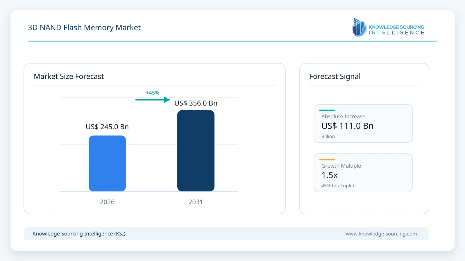
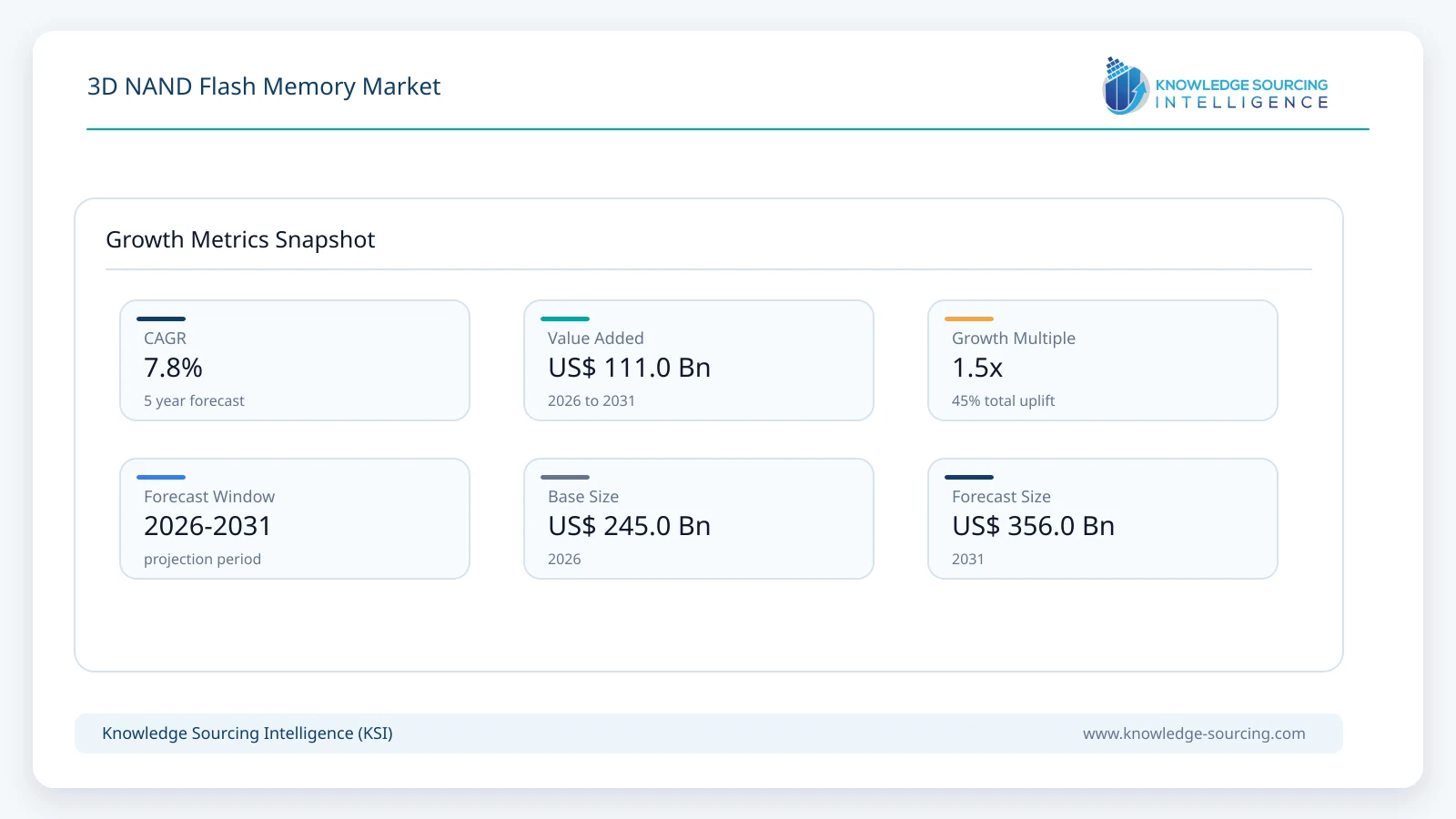
The global 3D NAND flash memory market is estimated at USD 245.0 billion in 2026 and is forecast to reach USD 356.0 billion by 2031, representing a CAGR of approximately 7.8% over the forecast period.
Highlights:
- 1TLC accounts for approximately 54% of the global 3D NAND flash memory market in 2026, retaining the largest share by technology.
- 2Data centers and enterprise storage represent the largest end-user segment in 2026, supported by AI infrastructure and high-capacity enterprise SSD deployment.
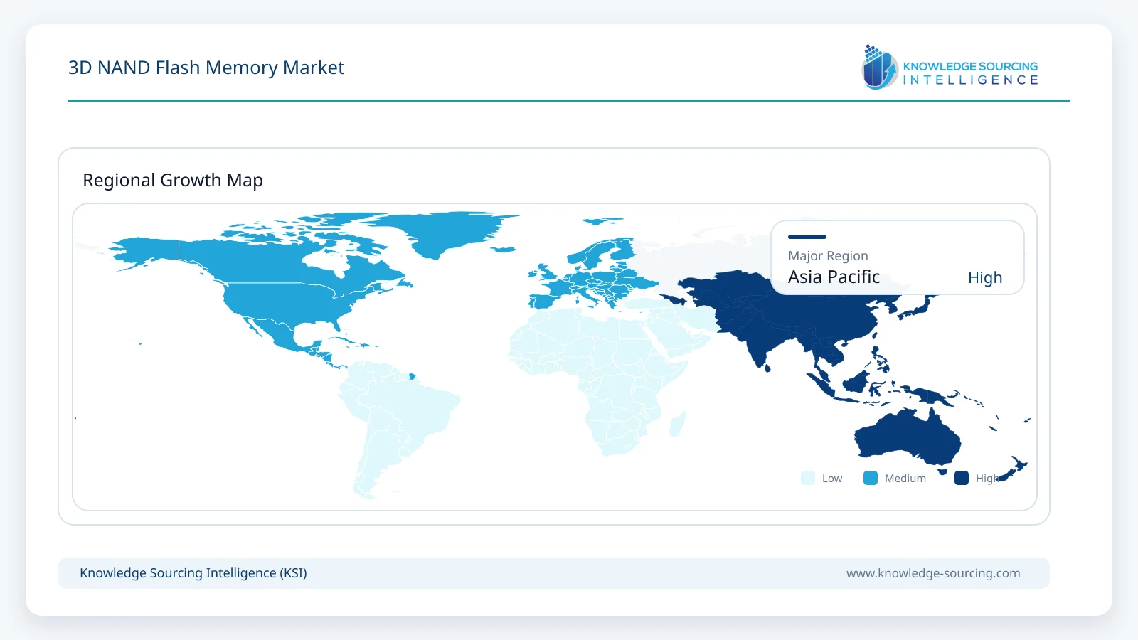
- 3Asia Pacific accounts for approximately 66% of the global market in 2026, supported by concentrated NAND manufacturing across South Korea, Japan, China and Singapore.
- 4QLC is expected to record the strongest expansion through 2031, supported by increasing adoption across high-capacity enterprise and client SSDs.
- 5300-layer-plus NAND is moving into commercial production, with current products exceeding 300 layers and next-generation architectures emphasizing density and cost per bit.
Key Highlights
3D NAND Flash Memory Market Overview
3D NAND flash memory has become the principal architecture used for high-density non-volatile semiconductor storage, replacing planar NAND across most high-volume applications by stacking memory cells vertically rather than attempting to increase density exclusively through horizontal process scaling. The technology supports smartphones, client and enterprise solid-state drives, data center storage, automotive systems, industrial electronics and embedded devices, while improvements in layer count, cell density and controller performance continue to reduce the physical area required for each stored bit. The market has moved well beyond the early 32-layer and 64-layer generations described in older industry research. Current commercial products include Samsung's ninth-generation V-NAND, SK hynix's 321-layer 4D NAND and Kioxia and SanDisk's tenth-generation BiCS technology, with manufacturers increasingly combining vertical scaling with lateral scaling, wafer bonding and advanced controller architectures. Samsung's ninth-generation V-NAND increased bit density by approximately 50% compared with its previous generation and supports interface speeds of up to 3.2Gbps.
The market environment in 2026 differs substantially from the conditions reflected in the previous KSI 3D NAND estimate. NAND demand has shifted toward high-capacity storage for AI infrastructure and enterprise servers while manufacturing capacity remains constrained. TrendForce reported that combined revenue of the top five NAND suppliers increased from approximately USD 21.17 billion in Q4 2025 to more than USD 38.9 billion in Q1 2026, before rising sharply again in Q2 2026. Because advanced 3D architectures account for the overwhelming majority of current high-volume NAND production, the legacy KSI estimate of USD 30.257 billion in 2025 is no longer compatible with observed supplier revenues or the current structure of the NAND industry. The revised 2026 estimate therefore reflects current supplier revenue, high 3D NAND penetration, enterprise storage demand and elevated NAND pricing rather than mechanically extending the previous 23.91% CAGR.
Major Market Drivers
AI Infrastructure Is Accelerating High-Capacity Enterprise SSD Demand
The build-out of AI computing infrastructure is creating a new demand profile for NAND storage. Training and inference systems require very large datasets to move efficiently between long-term storage, CPUs, GPUs and high-speed memory, increasing the importance of enterprise SSDs with high capacity, sustained throughput and lower power consumption per stored terabyte. TrendForce reported that enterprise SSD demand from cloud service providers accelerated sharply in the first quarter of 2026 as AI server deployment and shortages of conventional high-capacity HDDs shifted additional storage orders toward NAND-based solutions. Combined revenue of the five leading NAND suppliers consequently rose 83.7% quarter-on-quarter to more than USD 38.9 billion in Q1 2026.
The shift strengthened further during the second quarter. TrendForce reported that combined revenue of the leading enterprise SSD vendors approached USD 37.59 billion in Q2 2026 as both unit shipments and contract prices increased. Suppliers are responding with higher-density QLC products and new enterprise SSD platforms designed for AI and high-performance computing. Samsung began mass production of its PCIe 6.0 PM1763 enterprise SSD in July 2026 using ninth-generation V-NAND, while Kioxia's tenth-generation BiCS devices are being positioned primarily for enterprise and data center SSDs.
Higher Layer Counts Continue to Reduce Cost per Bit
Vertical scaling remains one of the principal mechanisms through which manufacturers increase NAND density and lower manufacturing cost per stored bit. Instead of relying exclusively on smaller lateral feature sizes, 3D NAND manufacturers stack additional memory-cell layers vertically while improving channel-hole etching, bonding and peripheral circuitry. Samsung's ninth-generation V-NAND increased bit density by approximately 50% compared with the previous generation while reducing power consumption by about 10%, demonstrating that higher density can be accompanied by improvements in performance and efficiency.
SK hynix has extended commercial layer counts beyond the 300-layer threshold. Its 321-layer TLC NAND entered mass production before being followed by a 321-layer 2Tb QLC product, while the company's PQC21 client SSD began shipping to Dell Technologies in April 2026 using 321-layer QLC NAND. The product is available in 1TB and 2TB configurations and is designed for AI PC storage. Kioxia and SanDisk are pursuing a different combination of vertical and lateral scaling through their BiCS10 architecture. The 1Tb TLC device reaches a density above 29Gb/mm² and improves bit density by 59% compared with BiCS8 while delivering a 33% higher interface speed.
QLC Adoption Is Expanding the Addressable Market for 3D NAND
Quad-level cell NAND is becoming increasingly important because it stores four bits per cell, enabling substantially higher storage capacity from the same physical silicon area. QLC historically faced endurance and performance limitations relative to TLC, but improvements in controller design, error correction, firmware and high-layer NAND architectures have made the technology increasingly viable for client and enterprise storage applications where capacity and cost per terabyte are critical.
SK hynix's 321-layer QLC roadmap illustrates the change. The company developed a 2Tb QLC NAND device with six independent planes to improve parallelism and performance and began supplying a 321-layer QLC client SSD to Dell Technologies in April 2026. SK hynix cited IDC data indicating that QLC could increase from 22% of the client SSD market in 2025 to 61% by 2027. Enterprise storage is moving in a similar direction as cloud operators adopt high-capacity QLC SSDs for data-intensive AI workloads and as HDD supply constraints make flash more attractive for selected storage tiers.
Device Storage Requirements Continue to Increase
AI infrastructure currently provides the strongest incremental demand, but consumer devices remain an important source of NAND bit consumption. Smartphones increasingly offer 256GB and 512GB base configurations, while premium devices frequently extend into 1TB storage capacities. AI PCs are similarly increasing local storage requirements as on-device models, higher-resolution media and AI-enabled productivity applications consume more capacity. The technical transition toward higher-density TLC and QLC products allows manufacturers to increase device capacity without proportionally increasing package size, which is particularly important for smartphones and thin notebook computers.
SK hynix's 321-layer QLC client SSD is specifically designed for AI PCs, while its advanced 321-layer TLC NAND is being deployed across mobile, PC and data center applications. Consumer electronics demand has been softer during parts of 2026 because elevated component prices increased device bill-of-material costs, but rising storage density per device continues to support long-term NAND bit demand even when unit shipment growth is moderate.
Major Market Restraints
NAND Pricing Remains Highly Cyclical
The NAND industry continues to experience pronounced supply-demand cycles because changes in wafer input, capacity utilization and process migration can produce large movements in bit supply, while demand varies across smartphones, PCs, enterprise servers and storage infrastructure. The 2026 market demonstrates the upside of this cycle. TrendForce reported severe supply tightness during the first half of the year, with NAND flash contract prices expected to increase another 10% to 15% quarter-on-quarter in Q3 2026 after exceptionally strong increases earlier in the year.
The same dynamics create downside risk when additional supply reaches the market. TrendForce expects NAND bit supply growth to begin exceeding demand growth in 2027 as manufacturers obtain greater output through process migration and weak consumer-electronics demand limits absorption. Supply constraints are therefore expected to ease during the second half of 2027. The 3D NAND market consequently cannot be evaluated using a smooth annual growth curve because increases in bit shipments can coincide with lower average selling prices, while periods of restricted output can produce strong revenue growth even when underlying device shipments remain moderate.
Manufacturing Complexity Rises With Layer Count
Adding memory layers improves density but also increases manufacturing complexity. High-aspect-ratio channel-hole etching becomes progressively more difficult as manufacturers attempt to create uniform vertical structures through hundreds of stacked layers. Process variation can reduce yields, while additional stacking and bonding steps increase the importance of equipment precision and defect control. Samsung uses advanced channel-hole etching and a double-stack architecture in its ninth-generation V-NAND, while SK hynix developed a multi-plug process to produce its 321-layer architecture.
Kioxia and SanDisk are addressing similar challenges through CMOS directly Bonded to Array technology, which manufactures the CMOS peripheral circuitry and memory-cell array separately before bonding them together. The approach improves density and performance but introduces additional process integration requirements. Capital requirements remain substantial because leading-edge NAND production depends on advanced etching, deposition, metrology and wafer-processing equipment alongside large cleanroom facilities.
High Memory Prices Are Constraining Consumer Demand
Strong server demand and restricted supply have improved supplier profitability but have simultaneously raised component costs for smartphone and PC manufacturers. TrendForce reported in July 2026 that consumer electronics brands were approaching their affordability limits after repeated memory price increases, contributing to weaker notebook and smartphone demand and a more subdued consumer peak season.
This creates a more polarized demand environment in which cloud service providers continue to procure high-capacity storage while consumer-device manufacturers manage inventories more conservatively. Suppliers have therefore been reallocating advanced capacity toward higher-margin enterprise applications rather than maximizing consumer-volume production.
Market Trends
Commercial Products Have Moved Beyond 300 Layers
The 300-layer threshold has moved from development roadmaps into commercial production. SK hynix began mass production of 321-layer TLC NAND and subsequently developed a 321-layer 2Tb QLC product, while commercial devices incorporating the technology entered the PC market during 2026. This transition matters because manufacturers can increase bit output through process migration without adding equivalent wafer capacity, which is particularly important when cleanroom space and capital budgets remain constrained.
The competitive focus is also shifting from layer count alone toward the combination of layer count, lateral scaling, interface speed, power efficiency and manufacturing yield. Kioxia and SanDisk's BiCS10 architecture illustrates this direction by combining advanced lateral scaling with CMOS bonding rather than relying solely on additional vertical layers. The 1Tb TLC device improves bit density by 59%, increases interface speed by 33% and reduces output power consumption by 34% compared with BiCS8.
CMOS Bonding Is Becoming More Important
Manufacturers increasingly separate peripheral CMOS circuitry from the NAND cell array to optimize each structure independently. Kioxia and SanDisk use CMOS directly Bonded to Array in their advanced BiCS generations, allowing logic and memory layers to be produced separately and bonded during manufacturing. Their tenth-generation products are entering production at the Kitakami Fab2 facility, which opened in September 2025 and began 10th-generation production in July 2026.
This architecture supports higher density and improved interface performance while providing another route for scaling as conventional vertical stacking becomes more difficult. Comparable approaches are becoming strategically important across the NAND industry because future density improvements will increasingly depend on combining vertical scaling with wafer bonding, lateral scaling and controller-level optimization.
Supplier Investment Is Returning, But New Capacity Arrives Gradually
NAND suppliers curtailed capacity additions during earlier downturns, contributing to the supply constraints visible in 2026. Investment is now returning, but new fabs require several years to construct and ramp. Micron's Singapore expansion is one of the clearest examples. The company plans to invest approximately USD 24 billion over ten years in a new NAND wafer fabrication facility that will eventually provide around 700,000 square feet of cleanroom space, with output scheduled to begin in the second half of 2028.
Kioxia and SanDisk are also expanding advanced production through Kitakami Fab2 in Japan. The facility began operating with eighth-generation BiCS technology before adding tenth-generation production in July 2026. These investments increase long-term bit supply, but near-term output growth still depends heavily on technology migration within existing wafer capacity.
Technological Outlook
3D NAND technology development through 2031 is expected to focus on higher effective layer counts, improved lateral density, wafer bonding, faster interfaces and greater use of QLC. Adding layers remains important, but manufacturers increasingly evaluate architecture according to usable bit density, manufacturing yield and cost rather than the headline layer number alone. Samsung's ninth-generation V-NAND, SK hynix's 321-layer NAND and Kioxia and SanDisk's BiCS10 demonstrate three different approaches to improving density and performance, with all three combining process scaling with architectural changes.
QLC is expected to capture a growing portion of high-capacity SSD demand, particularly where workload characteristics allow endurance to be managed through controller and firmware optimization. TLC remains critical for applications requiring a stronger balance of endurance, latency and density, while SLC and MLC retain specialized roles in industrial, automotive and other high-endurance applications. Beyond 300 layers, manufacturing economics will increasingly depend on high-aspect-ratio etching, multi-stack integration, CMOS bonding and yield management rather than layer count in isolation.
Segment Analysis:
By Technology
Triple-Level Cell (TLC)
TLC remains the largest technology category in the 3D NAND flash memory market in 2026, accounting for an estimated 54% of market value. The architecture stores three bits in each memory cell and provides a balance between capacity, endurance, cost and performance that allows it to serve smartphones, client SSDs, enterprise SSDs and other high-volume storage applications. Leading manufacturers continue to invest heavily in advanced TLC even as QLC adoption accelerates. Samsung's ninth-generation 1Tb TLC V-NAND entered mass production with approximately 50% higher bit density than the prior generation, while Kioxia's tenth-generation 1Tb TLC BiCS technology is being targeted primarily at enterprise and data center SSDs.
TLC's position is increasingly concentrated in applications where sustained performance and endurance justify a higher cost per bit than QLC. QLC is expected to capture a larger portion of capacity-oriented workloads through 2031, particularly enterprise storage and client SSDs, but TLC remains important for performance-sensitive storage tiers and premium mobile applications.
By End-User Industry
Data Centers and Enterprise Storage
Data centers and enterprise storage have become the largest value-generating end-user segment for 3D NAND in 2026, reflecting elevated enterprise SSD prices and rapid deployment of storage for AI infrastructure. TrendForce reported combined enterprise SSD revenue of approximately USD 37.59 billion among the five leading vendors in Q2 2026, more than double the previous quarter, as AI server deployment, cloud infrastructure expansion and higher contract prices increased supplier revenue. The segment's importance is also reflected in supplier product roadmaps. Samsung's PM1763 uses PCIe 6.0 and ninth-generation V-NAND for AI and HPC servers, SK hynix is expanding high-capacity QLC solutions through Solidigm, and Kioxia is directing its tenth-generation BiCS devices toward enterprise and data center SSDs.
The addition of Data Centers and Enterprise Storage as a separate segment is therefore necessary. Treating enterprise storage within an undifferentiated "Others" category, as in the legacy report, no longer represents the commercial structure of the 3D NAND market.
By Geography
Asia Pacific
Asia Pacific remains the largest regional market and production base for 3D NAND, accounting for an estimated 66% of global market value in 2026. South Korea hosts major Samsung and SK hynix NAND operations, Japan remains central through Kioxia and SanDisk's joint manufacturing infrastructure, China has developed substantial domestic capacity through YMTC, and Singapore is Micron's principal NAND manufacturing location. Micron stated that its new USD 24 billion Singapore facility will be built within its existing NAND manufacturing complex and will begin wafer output during the second half of 2028.
Japan is also receiving new advanced capacity. Kioxia and SanDisk began production of tenth-generation 3D flash products at Kitakami Fab2 in July 2026, strengthening Japan's position in advanced NAND manufacturing. Asia Pacific simultaneously contains large downstream electronics manufacturing industries across China, South Korea, Japan, Taiwan, India and Southeast Asia, connecting wafer fabrication with smartphone, computer, automotive and electronics supply chains.
Competitive Landscape
The 3D NAND flash memory market remains highly concentrated because advanced NAND fabrication requires substantial capital investment, proprietary process technology and long development cycles. Samsung Electronics remains the largest global NAND supplier and generated approximately USD 23.06 billion of NAND revenue in Q2 2026 according to TrendForce, while SK hynix Group, Micron, Kioxia and SanDisk form the other major publicly tracked suppliers. Competition increasingly centers on enterprise SSD exposure, high-layer NAND, QLC adoption, manufacturing yields and long-term access to cleanroom capacity rather than layer count alone.
The company structure has also changed materially from the legacy KSI report. Intel is no longer a current NAND manufacturer, following the transfer of its NAND and SSD business to SK hynix and the creation of Solidigm. Western Digital should no longer be listed as the current flash company following the separation of its flash business into SanDisk Corporation. Kioxia replaces the legacy Toshiba Memory identity as the relevant NAND company. The current competitive set therefore includes Samsung Electronics, SK hynix, Micron Technology, Kioxia, SanDisk and YMTC as the principal advanced NAND manufacturers, with Solidigm remaining strategically important in enterprise SSDs as part of the SK hynix group.
Recent Developments
July 2026: Kioxia and SanDisk began production of their tenth-generation 3D flash technology at Kitakami Fab2 in Japan. The facility is scaling production using CBA architecture to address higher demand for advanced NAND.
July 2026: SanDisk began sampling its BiCS10 1Tb TLC device with more than 29Gb/mm² density, a 59% improvement in bit density and up to 4.8Gb/s interface speed.
July 2026: Samsung began mass production of its PM1763 PCIe 6.0 enterprise SSD using ninth-generation V-NAND and a 4nm controller for AI and HPC server applications.
April 2026: SK hynix began supplying its PQC21 client SSD containing 321-layer QLC NAND, with 1TB and 2TB configurations and initial supply to Dell Technologies.
January 2026: Micron broke ground on a new NAND wafer fabrication facility in Singapore under an approximately USD 24 billion ten-year investment program. The facility will add around 700,000 square feet of cleanroom space.
August 2025: SK hynix began mass production of its 321-layer 2Tb QLC NAND, the first commercially announced QLC NAND implementation above 300 layers.
Market Outlook
The 3D NAND market through 2031 will be shaped by two overlapping forces: sustained expansion in the number of NAND bits required by AI, enterprise storage and higher-capacity devices, and continued volatility in the price paid for those bits. The 2026 shortage has created unusually strong supplier revenues, but current conditions are unlikely to translate into a uniform annual revenue trajectory. TrendForce expects supply growth to exceed demand growth during 2027 as process migrations increase bit output and consumer demand remains comparatively weak, suggesting that pricing could soften even while physical NAND consumption continues rising.
Beyond this near-term normalization, enterprise storage, AI PCs, larger smartphone capacities, software-defined vehicles and industrial edge systems provide a broad base for higher NAND bit consumption. Manufacturing will continue shifting toward 300-layer-plus architectures, advanced QLC, CMOS bonding and higher-speed interfaces, while older planar NAND remains concentrated in specialized legacy applications.
3D NAND Flash Memory Market Scope:
| Report Metric | Details |
|---|---|
| Total Market Size in 2026 | USD 245.0 billion |
| Total Market Size in 2031 | USD 356.0 billion |
| Forecast Unit | USD Billion |
| Growth Rate | 7.8% |
| Study Period | 2021 to 2031 |
| Historical Data | 2021 to 2024 |
| Base Year | 2025 |
| Forecast Period | 2026 – 2031 |
| Segmentation | Type, End-User Industry, Geography |
| Companies |
|
Market Segmentation
By Technology
Single-Level Cell (SLC)
Multi-Level Cell (MLC)
Triple-Level Cell (TLC)
Quad-Level Cell (QLC)
By End-User Industry
Data Centers and Enterprise Storage
Automotive
Consumer Electronics
Communications
Industrial and Other Applications
By Geography
North America
United States
Canada
Mexico
South America
Brazil
Argentina
Others
Europe
Germany
France
United Kingdom
Others
Middle East and Africa
Saudi Arabia
Israel
Others
Asia Pacific
China
Japan
India
South Korea
Taiwan
Others
Table of Contents
1. INTRODUCTION
1.1. Market Overview
1.2. Market Definition
1.3. Scope of the Study
1.4. Market Segmentation
1.5. Currency
1.6. Assumptions
1.7. Base and Forecast Years Timeline
1.8. Key Benefits for Stakeholders
2. RESEARCH METHODOLOGY
2.1. Research Design
2.2. Research Process
2.3. Primary Research
2.4. Secondary Research
2.5. Market Estimation
2.6. Data Triangulation
2.7. Forecast Methodology
3. EXECUTIVE SUMMARY
3.1. Key Findings
3.2. Analyst View
4. BUSINESS LANDSCAPE
4.1. Market Drivers
4.1.1. Expansion of AI Infrastructure and Enterprise SSD Demand
4.1.2. Increasing 3D NAND Layer Counts and Bit Density
4.1.3. Expansion of QLC Across Client and Enterprise Storage
4.1.4. Increasing Storage Capacity Across Connected Devices
4.2. Market Restraints
4.2.1. NAND Pricing and Supply-Demand Cyclicality
4.2.2. Increasing Manufacturing Complexity and Yield Requirements
4.2.3. Consumer Electronics Demand Sensitivity to Memory Prices
4.3. Market Opportunities
4.4. Porter's Five Forces Analysis
4.5. Industry Value Chain Analysis
4.6. NAND Supply, Capacity and Pricing Trends
4.7. Policies, Export Controls and Semiconductor Manufacturing Incentives
4.8. Strategic Recommendations
5. TECHNOLOGICAL OUTLOOK
5.1. Evolution of 3D NAND Layer Counts
5.2. 300-Layer-Plus NAND Architectures
5.3. CMOS Bonding and Peripheral Circuit Integration
5.4. TLC and QLC Technology Roadmap
5.5. NAND Interface and Controller Development
5.6. Cost-per-Bit and Manufacturing Yield Outlook
6. 3D NAND FLASH MEMORY MARKET BY TECHNOLOGY
6.1. Introduction
6.2. Single-Level Cell (SLC)
6.3. Multi-Level Cell (MLC)
6.4. Triple-Level Cell (TLC)
6.5. Quad-Level Cell (QLC)
7. 3D NAND FLASH MEMORY MARKET BY END-USER INDUSTRY
7.1. Introduction
7.2. Data Centers and Enterprise Storage
7.3. Automotive
7.4. Consumer Electronics
7.5. Communications
7.6. Industrial and Other Applications
8. 3D NAND FLASH MEMORY MARKET BY GEOGRAPHY
8.1. North America
8.1.1. United States
8.1.2. Canada
8.1.3. Mexico
8.2. South America
8.2.1. Brazil
8.2.2. Argentina
8.2.3. Others
8.3. Europe
8.3.1. Germany
8.3.2. France
8.3.3. United Kingdom
8.3.4. Others
8.4. Middle East and Africa
8.4.1. Saudi Arabia
8.4.2. Israel
8.4.3. Others
8.5. Asia Pacific
8.5.1. China
8.5.2. Japan
8.5.3. India
8.5.4. South Korea
8.5.5. Taiwan
8.5.6. Others
9. COMPETITIVE INTELLIGENCE
9.1. Major Players and Strategy Analysis
9.2. Advanced 3D NAND Technology Roadmaps
9.3. Manufacturing Capacity and Investment Analysis
9.4. Mergers, Agreements and Technology Partnerships
9.5. Vendor Competitiveness Matrix
10. COMPANY PROFILES
10.1. Samsung Electronics Co., Ltd.
10.2. SK hynix Inc.
10.3. Micron Technology, Inc.
10.4. Kioxia Corporation
10.5. SanDisk Corporation
10.6. Yangtze Memory Technologies Co., Ltd.
10.7. Solidigm
10.8. ATP Electronics, Inc.
Navigate
Trusted by the world's leading organizations











