
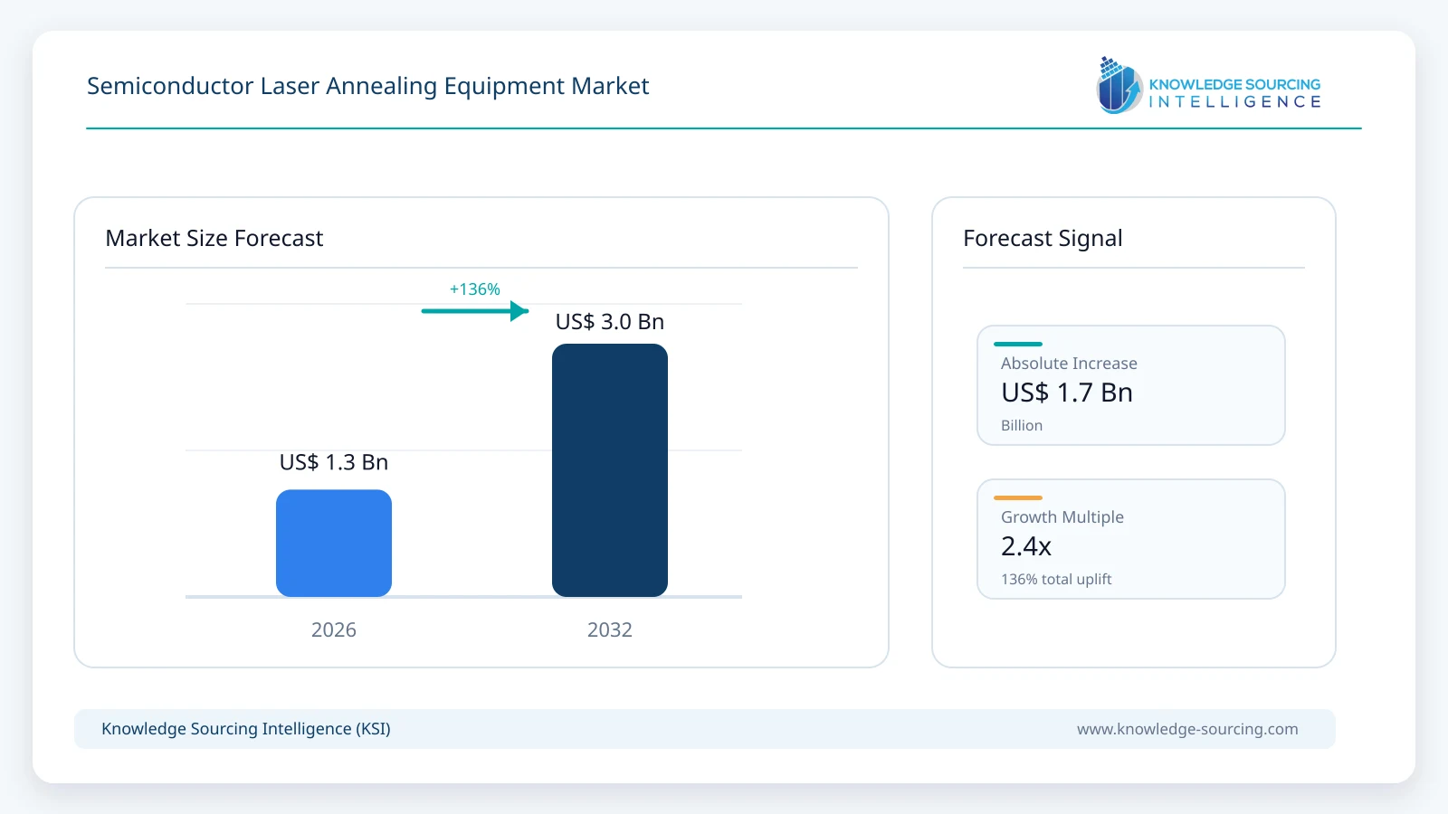
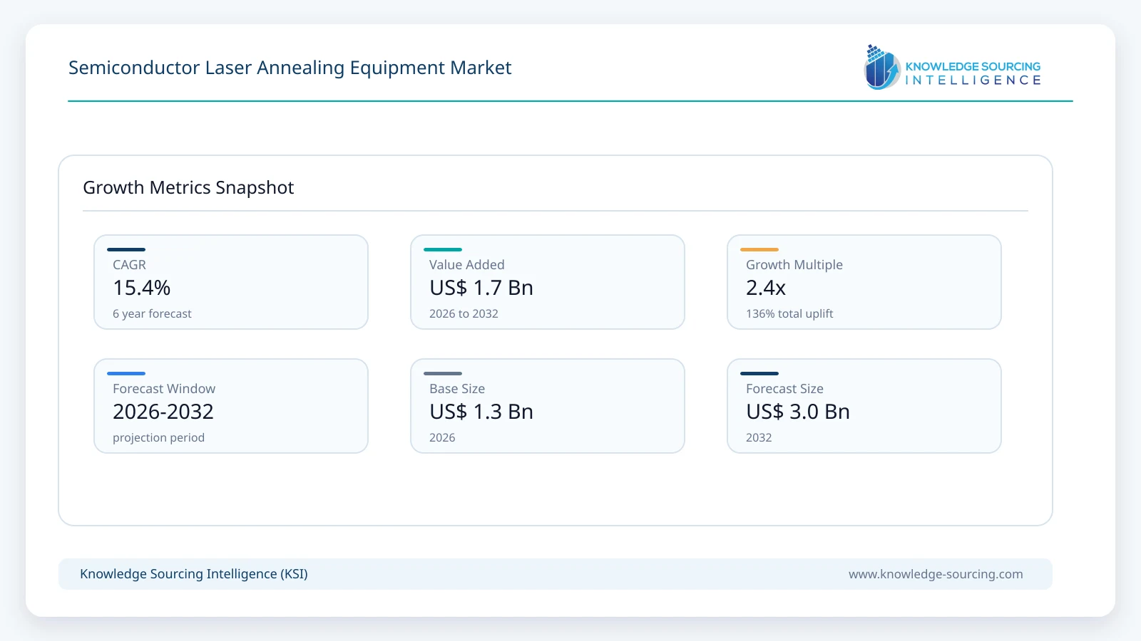
The Semiconductor Laser Annealing Equipment Market is estimated at USD 1.25 billion in 2026 and is projected to reach USD 2.95 billion by 2032, representing a CAGR of 15.4% during 2026-2032.
Highlights:
- 1Nanosecond and microsecond systems gain importance as advanced devices require high activation with lower thermal budgets.
- 2Gate-all-around logic and stacked device architectures expand demand for shallow, localized thermal processing.
- 3Laser annealing adoption is broadening into high-layer NAND and silicon-carbide power-semiconductor manufacturing.
- 4UV, green and excimer architectures coexist because absorption depth, thermal penetration and wafer material differ by application.
- 5Asia Pacific remains the largest opportunity because Japan, South Korea, Taiwan and China combine leading fabs with a strong local equipment ecosystem.
Market Overview
Laser annealing replaces or supplements conventional furnace and rapid thermal annealing when the process requires extremely short heating cycles or highly localized energy deposition. The laser beam can be shaped into a line, spot or broad area and scanned across the wafer so that the surface reaches a high peak temperature while deeper device layers remain comparatively cool. This is particularly useful for source/drain activation, contact engineering, thin-film crystallization and material modification near temperature-sensitive structures.
The time scale determines how heat moves through the wafer. Millisecond laser-spike annealing allows relatively deeper thermal diffusion while maintaining a lower overall thermal budget than furnace processing. Nanosecond systems confine heat much closer to the surface and are suited to shallow activation, stacked-device processing and material modification. Microsecond ultraviolet systems offer an intermediate regime and can be tuned for silicon as well as wide-bandgap materials. Excimer-laser platforms provide short-wavelength, high-energy pulses with shallow optical absorption and are used where strong surface interaction and precise pulse control are required.
The equipment challenge is not simply generating laser power. Production systems must maintain energy-density uniformity across 200 mm or 300 mm wafers, manage wafer warpage and reflectivity, align the scan without overlap defects, control thermal history and prevent contamination from laser-induced fumes. Beam homogenization, wafer transport, temperature metrology, recipe control and chamber atmosphere therefore become as important as the laser source itself. These requirements keep the market concentrated among specialist suppliers with deep process-integration capability.
Market Drivers
Advanced logic requires lower thermal-budget activation
Gate-all-around transistors, nanosheet structures and increasingly complex contact stacks reduce the temperature margin available for post-implant annealing. Veeco's NSA500 is being evaluated by multiple advanced-logic customers because nanosecond dwell times can activate dopants and modify materials without exposing underlying structures to long thermal cycles. As logic moves beyond 2 nm, localized annealing becomes increasingly attractive for process steps where diffusion control and thermal isolation are critical.
High-layer NAND increases demand for localized crystallization and repair
Three-dimensional NAND stacks continue to increase in layer count, producing deeper channel structures and more difficult thermal-process requirements. Localized laser heating can support crystallization, defect repair and process tuning while limiting heat exposure across the full stack. Industry activity during 2026 increasingly linked laser annealing with 400-layer-class NAND development, widening the opportunity beyond logic.
SiC and GaN expand the addressable equipment base
Wide-bandgap power semiconductors require very high activation temperatures and specialized contact engineering. Silicon carbide can require thermal conditions above those used for silicon, while prolonged heating can damage interfaces or introduce unwanted diffusion. Short-duration laser processing can deliver high local energy for activation, silicidation and ohmic-contact formation while limiting bulk-wafer heating. Sumitomo Heavy Industries Material Solutions and JSW Aktina both position current laser systems for SiC applications, and 2026 industry activity indicates that power-semiconductor manufacturers are evaluating broader deployment.
Higher-value process integration favors production-qualified platforms
Leading fabs do not purchase annealing systems solely on peak laser output. Production adoption depends on within-wafer uniformity, wafer-per-hour throughput, overlap control, uptime, process monitoring, laser-source lifetime and repeatability across thousands of wafers. Suppliers with process-development labs, established field service and close relationships with foundries and memory manufacturers are therefore better positioned as laser annealing moves from evaluation into high-volume manufacturing.
Restraints and Adoption Challenges
Laser annealing remains more application-specific than conventional thermal processing. Reflectivity, absorption depth, film stack, wafer material and implanted species all affect the process window, so a recipe developed for one device may not transfer directly to another. High-power optical systems also require precise beam homogenization and regular calibration. Local melting or excessive thermal gradients can create defects if energy density is not tightly controlled. In addition, fabs already have mature rapid thermal and furnace processes, so laser systems must demonstrate a clear yield, performance or thermal-budget advantage before replacing installed equipment.
Segment Analysis
By Annealing Architecture
Nanosecond annealing is moving rapidly into advanced-node logic because the extremely short thermal pulse helps limit diffusion and protect temperature-sensitive three-dimensional structures. Millisecond laser-spike platforms remain important where a somewhat deeper heat profile is required, while microsecond ultraviolet systems provide process flexibility across silicon and wide-bandgap semiconductors. Excimer platforms are particularly relevant for shallow surface processing, activation and silicidation, and point-scanning systems are being developed to improve overlap control and wafer uniformity.
Application requirements differ materially. Logic customers prioritize shallow activation, contact engineering and low thermal budget. Memory customers require uniformity across complex three-dimensional stacks. Image-sensor manufacturers use localized activation to preserve surrounding structures, while SiC and GaN manufacturers focus on activation, silicidation and ohmic-contact formation at temperatures that are difficult to achieve efficiently with conventional processes.
Technology | Typical Time Scale | Primary Applications | Commercial Direction |
Nanosecond annealing | Nanoseconds | Advanced logic, stacked devices, shallow activation | Strongest momentum in leading-edge logic and memory |
Laser-spike / millisecond | Milliseconds | Dopant activation, contact engineering, advanced CMOS | Established production technology with continued node migration |
Microsecond UV annealing | Microseconds | Activation, crystallization, SiC/GaN processing | Expanding across silicon and wide-bandgap devices |
Excimer laser annealing | Tens of nanoseconds | Surface activation, silicidation, image sensors, SiC | Growing in specialized high-energy surface processes |
Point / spot scanning | Application dependent | DRAM, NAND, localized activation | Emerging route to reduce scan-overlap defects |
Line-beam scanning | Application dependent | High-throughput surface annealing | Favored where uniform large-area exposure is required |
Market and Technology Indicators
Indicator | Current Evidence | Market Impact |
Advanced-logic qualification | Veeco received a follow-on NSA500 order in June 2026 after customer acceptance of an evaluation tool. | Shows nanosecond annealing moving from evaluation toward repeat production orders. |
Third logic-customer evaluation | Veeco shipped an NSA500 to another advanced-logic customer for evaluation, with completion expected in 2027. | Broadens the potential installed base beyond the initial customer set. |
Microsecond UV platform | Sumitomo Heavy Industries Material Solutions offers the QA-3000 for silicon, SiC and GaN. | Expands laser annealing into wider material systems and thermal-budget regimes. |
SiC silicidation equipment | JSW Aktina markets YIELDSCAN platforms for SiC silicidation and activation. | Creates a dedicated equipment opportunity in power semiconductors. |
SiC and NAND adoption | 2026 industry reports linked laser annealing with SiC production and 400-layer NAND development. | Supports demand beyond advanced logic. |
300 mm point-scanning systems | RNR Lab positions the ALP-300M for next-generation DRAM and V-NAND. | Adds a localized scanning architecture aimed at high-volume memory manufacturing. |
Regional Opportunity
Asia Pacific
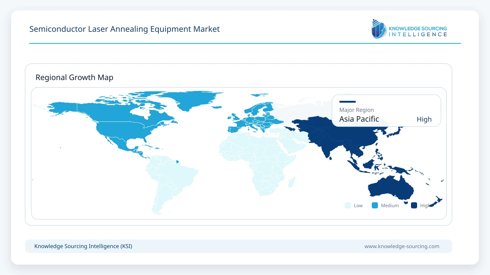
Asia Pacific is the largest market for semiconductor laser annealing equipment because it combines the highest concentration of advanced logic, memory, image-sensor and power-semiconductor production. Taiwan and South Korea are central through leading-edge foundry, DRAM and NAND manufacturing, while Japan has an unusually strong domestic supplier base in laser-annealing systems, precision optics, laser sources and wafer-processing equipment. China adds a growing installed base of logic, memory and power-semiconductor fabs and is investing in domestic process-equipment capability.
Japan is particularly important on the supply side. Sumitomo Heavy Industries Material Solutions offers nanosecond and microsecond laser platforms, including the QA-3000, while JSW Aktina provides semiconductor laser systems for activation, silicidation and related Si/SiC processes. These suppliers benefit from proximity to Japanese power-semiconductor manufacturers, image-sensor production and advanced materials expertise. Their product portfolios also illustrate how the market is diversifying beyond silicon CMOS into SiC, GaN and specialty devices.
South Korea is important through Samsung Electronics, SK hynix and a growing domestic equipment ecosystem. RNR Lab is developing 300 mm point-scanning laser-annealing systems for DRAM and V-NAND, while AP Systems has longstanding excimer-laser expertise across electronic-device manufacturing. Taiwan remains central because leading foundry and advanced-packaging capacity creates demand for thermal processes compatible with aggressive node scaling. China is likely to expand both demand and domestic equipment participation as local fabs increase process complexity.
North America remains strategically important because leading-edge logic customers are evaluating and ordering Veeco nanosecond annealing systems. Europe contributes through specialty semiconductor and power-device manufacturing as well as laser-source and optics suppliers. The region is smaller in wafer volume than Asia Pacific but relevant for SiC, automotive semiconductors and laser-system technology.
Competitive Landscape
The competitive landscape is relatively concentrated because production laser annealing requires tightly integrated optics, motion control, wafer handling, thermal modeling and process know-how. Veeco is a major supplier in advanced logic and memory through laser-spike and nanosecond annealing platforms. Sumitomo Heavy Industries Material Solutions participates across nanosecond, microsecond and solid-state laser systems, while JSW Aktina competes in excimer-laser activation and SiC silicidation applications.
RNR Lab is emerging in South Korea with high-speed point-scanning equipment targeted at DRAM and V-NAND. AP Systems brings extensive excimer-laser and electronic-device manufacturing experience. The wider ecosystem includes Coherent, TRUMPF, MKS Instruments / Spectra-Physics, IPG Photonics and other laser-source or beam-delivery suppliers whose products can be integrated into semiconductor thermal-processing platforms. Competitive differentiation increasingly depends on thermal-budget control, within-wafer uniformity, scan-overlap management, throughput, process repeatability, uptime and field support.
Major companies and ecosystem participants covered: Veeco Instruments, Sumitomo Heavy Industries Material Solutions, JSW Aktina System, RNR Lab, AP Systems, Coherent, TRUMPF, MKS Instruments / Spectra-Physics, IPG Photonics, Han's Laser, EO Technics, SCREEN Semiconductor Solutions, Gigaphoton, Cymer / ASML and ESI / MKS Instruments.
Recent Developments
June 2026: Veeco received a follow-on NSA500 nanosecond annealing order from a leading logic customer after successful evaluation and customer acceptance.
June 2026: Veeco shipped an NSA500 system to a third advanced-logic customer for evaluation, extending its qualification pipeline for next-generation devices.
June 2026: Industry reports indicated broader laser-annealing evaluation for SiC power semiconductors and high-layer-count NAND, including interest around 8-inch SiC production.
August 2026: JSW Aktina announced that it would showcase semiconductor laser-annealing solutions for Si and SiC at ICSCRM 2026 and IIT 2026.
2026: Sumitomo Heavy Industries Material Solutions continued to promote the QA-3000 microsecond UV laser-annealing platform for silicon, SiC and GaN applications.
2026: RNR Lab continued development and commercialization of its ALP-300M 300 mm point-scanning laser-annealing platform for DRAM and V-NAND.
Semiconductor Laser Annealing Equipment Market Scope:
| Report Metric | Details |
|---|---|
| Total Market Size in 2026 | USD 1.25 billion |
| Total Market Size in 2032 | USD 2.95 billion |
| Forecast Unit | Billion |
| Growth Rate | 15.4% |
| Study Period | 2021 to 2032 |
| Historical Data | 2021 to 2024 |
| Base Year | 2025 |
| Forecast Period | 2026 – 2032 |
| Segmentation | Annealing Architecture, Laser Source, Application, Semiconductor Device, Wafer Size, Geography |
| Companies |
|
Market Segmentation
By Annealing Architecture
Nanosecond Laser Annealing
Laser-Spike / Millisecond Annealing
Microsecond UV Annealing
Excimer Laser Annealing
Point-Scanning Systems
Line-Beam Systems
By Laser Source
UV Solid-State Lasers
Green Lasers
Excimer Lasers
Infrared Lasers
Multi-Wavelength and Hybrid Systems
By Application
Dopant Activation
Source/Drain and Contact Engineering
Crystallization and Defect Repair
Silicidation and Ohmic-Contact Formation
Material Modification
Specialty and R&D Applications
By Semiconductor Device
Logic and Foundry Devices
DRAM
3D NAND
Image Sensors
Silicon-Carbide Power Devices
GaN and Other Compound Semiconductors
By Wafer Size
300 mm
200 mm
150 mm and Below
By Geography
Asia Pacific
Taiwan
South Korea
Japan
China
North America
United States
Europe
Rest of World
Table of Contents
1. EXECUTIVE SUMMARY
1.1. Market Opportunity and Key Findings
1.2. Laser Thermal-Budget Outlook
1.3. Advanced Logic, Memory and Power-Semiconductor Adoption
2. MARKET OVERVIEW
2.1. Semiconductor Laser-Annealing Process
2.2. Nanosecond, Microsecond and Millisecond Thermal Regimes
2.3. Beam Delivery, Homogenization and Wafer Scanning
2.4. Dopant Activation and Lattice Repair
2.5. Silicidation, Crystallization and Material Modification
3. MARKET SIZE AND FORECAST, 2026-2032
3.1. Global Market Revenue
3.2. Annual Growth Analysis
3.3. Equipment, Service and Process-Development Revenue
4. MARKET BY ANNEALING ARCHITECTURE
4.1. Nanosecond Laser Annealing
4.2. Laser-Spike / Millisecond Annealing
4.3. Microsecond UV Annealing
4.4. Excimer Laser Annealing
4.5. Point-Scanning Systems
4.6. Line-Beam Systems
5. MARKET BY LASER SOURCE
5.1. UV Solid-State Lasers
5.2. Green Lasers
5.3. Excimer Lasers
5.4. Infrared Lasers
5.5. Multi-Wavelength and Hybrid Systems
6. MARKET BY APPLICATION
6.1. Dopant Activation
6.2. Source/Drain and Contact Engineering
6.3. Crystallization and Defect Repair
6.4. Silicidation and Ohmic-Contact Formation
6.5. Material Modification
6.6. Specialty and R&D Applications
7. MARKET BY SEMICONDUCTOR DEVICE
7.1. Logic and Foundry Devices
7.2. DRAM
7.3. 3D NAND
7.4. Image Sensors
7.5. Silicon-Carbide Power Devices
7.6. GaN and Other Compound Semiconductors
8. MARKET BY WAFER SIZE
8.1. 300 mm
8.2. 200 mm
8.3. 150 mm and Below
9. REGIONAL MARKET
9.1. Asia Pacific
9.1.1. Taiwan
9.1.2. South Korea
9.1.3. Japan
9.1.4. China
9.2. North America
9.2.1. United States
9.3. Europe
9.4. Rest of World
10. MARKET DYNAMICS
10.1. Drivers
10.1.1. Advanced Logic Thermal-Budget Reduction
10.1.2. High-Layer NAND Processing
10.1.3. SiC and GaN Activation Requirements
10.1.4. Production Qualification of Localized Annealing
10.2. Restraints
10.2.1. Application-Specific Process Windows
10.2.2. Beam Uniformity and Calibration Requirements
10.2.3. High Capital and Optical-System Cost
10.2.4. Competition from Mature RTP and Furnace Processes
11. COMPETITIVE LANDSCAPE
11.1. Market Structure and Competitive Intensity
11.2. Nanosecond and Laser-Spike Platforms
11.3. Excimer and Microsecond UV Systems
11.4. SiC and Wide-Bandgap Strategies
11.5. Laser Sources, Optics and Process Integration
12. COMPANY PROFILES
12.1 Veeco Instruments
12.2 Sumitomo Heavy Industries Material Solutions
12.3 JSW Aktina System
12.4 RNR Lab
12.5 AP Systems
12.6 Coherent
12.7 TRUMPF
12.8 MKS Instruments / Spectra-Physics
12.9 IPG Photonics
12.10 Han's Laser
12.11 EO Technics
12.12 SCREEN Semiconductor Solutions
12.13 Gigaphoton
12.14 Cymer
12.15 MKS Instruments
13. RECENT DEVELOPMENTS
14. Appendix
Navigate
Trusted by the world's leading organizations











