
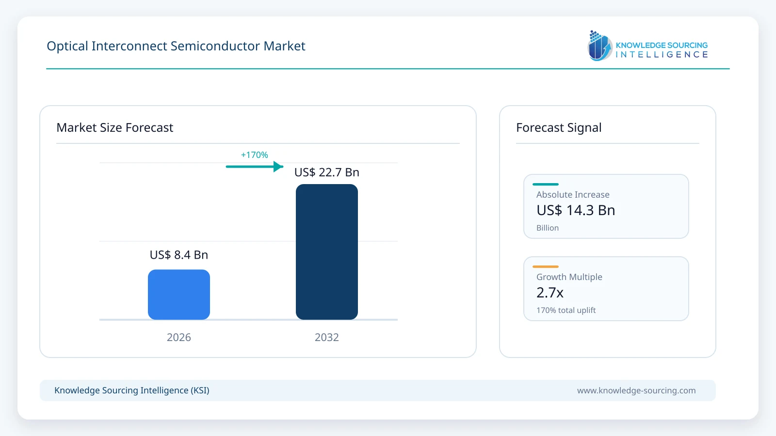
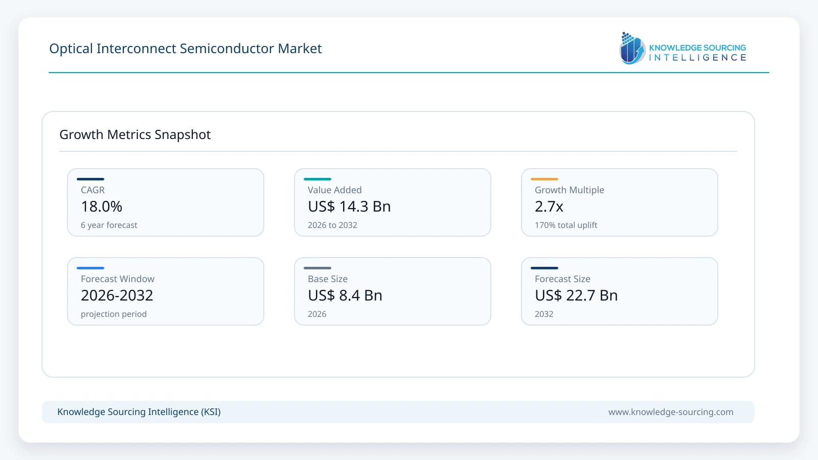
The Optical Interconnect Semiconductor Market is estimated at USD 8.40 billion in 2026 and is projected to reach USD 22.70 billion by 2032, representing a CAGR of 18.0% across 2026-2032.
Highlights:
- 1Optical DSPs remain the largest near-term semiconductor revenue pool in high-speed pluggable interconnects.
- 2Silicon photonics gains strategic importance as bandwidth density and optical integration move closer to compute.
- 3InP lasers and EMLs remain essential where high optical power and 200G-to-400G-per-lane performance are required.
- 4Optical input/output chiplets and CPO engines emerge fastest from a small commercial base.
- 5AI scale-up and scale-out networks are shifting optical design priorities toward lower power per bit and higher density.
The optical interconnect semiconductor stack converts high-speed electrical data into optical signals, transports those signals across fiber, and converts them back into electrical form at the receiving end. In a conventional pluggable transceiver, a host electrical interface connects to a DSP that performs equalization, clock recovery, forward error correction and modulation functions. Drivers then operate lasers or modulators, while photodiodes and TIAs recover the received optical signal. Silicon photonics integrates modulators, waveguides, multiplexers and photodetectors on a silicon-compatible platform, while InP remains important for efficient laser generation, electro-absorption modulation and optical amplification.
Artificial intelligence infrastructure is changing where these functions are physically placed. Traditional pluggable optics position the optical module at the front panel of a switch or accelerator system. Near-packaged optics shorten the electrical distance between switch silicon and the optical engine. Co-packaged optics place optical engines adjacent to the switching or compute silicon itself, reducing the length and power of high-speed electrical SerDes links. Optical input/output approaches move integration closer again by using compact optical chiplets that can be incorporated within advanced semiconductor packages. These architectures do not eliminate pluggable optics; instead, they create multiple semiconductor revenue pools differentiated by reach, bandwidth density, serviceability and power requirements.
The technology mix therefore remains heterogeneous. Silicon photonics is well suited to dense integration and wavelength-division multiplexing, but efficient on-chip light generation remains difficult in silicon, sustaining demand for external or hybrid InP lasers. InP EMLs continue to offer strong high-speed performance for 200G- and emerging 400G-per-lane links. GaAs VCSEL arrays remain relevant for short-reach multimode applications and highly parallel optical fabrics. The commercial winners are likely to be suppliers that combine photonics, high-speed analog electronics, packaging and manufacturing yield rather than relying on a single material platform.
Market Drivers
AI fabrics are increasing bandwidth density faster than electrical interconnect efficiency improves
AI clusters scale performance by connecting very large numbers of accelerators, memory resources and switches. As aggregate fabric bandwidth rises, high-speed copper links face increasing insertion loss, equalization complexity and power consumption over longer reaches. Optical links become more attractive when data must move across boards, racks and increasingly between compute trays inside dense scale-up systems. Broadcom, Marvell, Coherent and Lumentum are all developing 400G-per-lane technologies because the industry must increase bandwidth without allowing transceiver count and electrical power to rise proportionally.
The transition from 1.6T to 3.2T raises semiconductor content per optical port
The move from 800G to 1.6T initially increases demand for 200G-per-lane DSP, driver, TIA, laser and detector technologies. The next transition toward 3.2T introduces 400G-per-lane signaling and tighter requirements around analog bandwidth, modulation efficiency, photodiode performance and packaging parasitics. Marvell announced 2nm 400G-per-lane optical demonstrations in September 2026, while Coherent and Lumentum demonstrated 400G-class EML and photodiode technologies during 2026. Each speed transition therefore creates a semiconductor replacement cycle across the optical signal chain.
CPO and optical I/O address power and reach constraints near high-radix switches and accelerators
Moving optical engines closer to switch or compute silicon shortens power-hungry electrical links and can increase front-panel bandwidth density. GlobalFoundries introduced its SCALE CPO platform in May 2026, while Broadcom demonstrated 102.4T Ethernet switching with co-packaged optics. Intel continues to develop optical compute interconnect chiplets that combine silicon photonics with complementary metal-oxide-semiconductor electronics. These approaches expand the semiconductor opportunity from discrete transceiver components toward package-level optical engines and chiplets.
Foundry and packaging investment is reducing barriers to photonic integration
Optical interconnects require repeatable manufacturing across photonics wafers, electronic integrated circuits, laser attach, fiber coupling and advanced packaging. GlobalFoundries is investing in silicon photonics, novel optical materials and three-dimensional hybrid bonding under its 2026 CHIPS research and development program. Marvell, Broadcom, Intel and other suppliers are also integrating photonics with increasingly advanced electronic process nodes. Better process design kits, wafer-scale testing and packaging automation reduce the risk of scaling optical technologies from demonstration into volume production.
Restraints and Adoption Challenges
The largest constraints are packaging cost, thermal management, laser reliability and manufacturing yield. Optical engines require precise fiber alignment and low-loss coupling, while co-packaged architectures can complicate field replacement because optical components sit closer to high-value switch or compute silicon. External laser sources improve serviceability in some CPO designs but introduce additional fiber routing and redundancy requirements. Technology fragmentation also remains significant: silicon photonics, InP EMLs, VCSELs and emerging modulation platforms can each be optimal for different distances and power envelopes. Finally, standards for optical compute interconnects and package-level optical I/O are still maturing, so hyperscalers and semiconductor vendors may use proprietary architectures before a broad interoperable merchant ecosystem develops.
Optical Interconnect Semiconductor Market Segment Analysis
By Semiconductor Function
Optical DSP and associated high-speed analog interface integrated circuits represent the largest commercial semiconductor pool in 2026 because virtually every high-volume 800G and 1.6T pluggable architecture requires sophisticated signal processing, forward error correction and analog front-end functionality. Marvell and Broadcom have established large optical DSP portfolios, while other suppliers participate in drivers, TIAs and related connectivity silicon. Demand rises with both port count and lane speed, although linear pluggable and direct-drive architectures seek to reduce DSP power in selected short-reach deployments.
Optical I/O chiplets and co-packaged optical engines are expected to grow fastest through 2032 from a much smaller base. Their value proposition improves as electrical SerDes power and reach become more problematic at 200G- and 400G-per-lane host interfaces. Adoption will initially concentrate in high-radix AI switching and large accelerator fabrics where power savings and bandwidth density justify more complex packaging. Silicon photonics is a central integration platform for these products, while InP and other compound-semiconductor light sources remain important to the complete optical engine.
Technology Platform | Commercial Role | 2026-2032 Direction | Primary Use |
Optical DSPs and analog front ends | Signal conditioning, FEC, modulation, receive recovery | Strong | 800G, 1.6T and emerging 3.2T pluggables |
Silicon photonics PICs | Integrated modulation, multiplexing and photodetection | Very strong | Pluggables, CPO, NPO and optical I/O |
InP lasers and EMLs | High-power light sources and high-speed modulation | Very strong | 1.6T/3.2T modules, external lasers and coherent links |
GaAs VCSEL arrays | Parallel short-reach optical transmission | Strong | Scale-up and multimode high-density links |
Photodiodes, drivers and TIAs | Transmit/receive analog conversion | Strong | All major optical-link architectures |
Optical I/O / CPO semiconductor engines | Package-level optical connectivity | Fastest | AI scale-up, switch fabrics and future compute I/O |
Market and Technology Indicators
Indicator | Recent Development | Market Impact |
400G-per-lane optical roadmap | Marvell announced 2nm 400G/lane optical PAM4 demonstrations for ECOC 2026. | Supports the transition toward 3.2T pluggables and denser AI fabrics. |
CPO at 102.4T switching | Broadcom showcased a 102.4T Ethernet switch platform with co-packaged optics at OFC 2026. | Moves optical semiconductor content closer to switch silicon. |
Silicon photonics manufacturing investment | GlobalFoundries announced an expected USD 300 million U.S. CHIPS R&D award for next-generation silicon photonics. | Improves domestic process, packaging and scale-up capability for optical engines. |
1.6T and 3.2T component readiness | Coherent demonstrated silicon photonics, InP and VCSEL technologies spanning 1.6T and emerging 3.2T links. | Broadens the component ecosystem across multiple material platforms. |
Advanced modulator consolidation | Marvell acquired Polariton Technologies in April 2026. | Adds low-power high-speed modulation capability to integrated optical roadmaps. |
Optical compute I/O | Intel continues development of OCI chiplets with multi-terabit optical connectivity. | Creates a path from network optics toward package-level compute interconnect. |
Regional Opportunity
North America
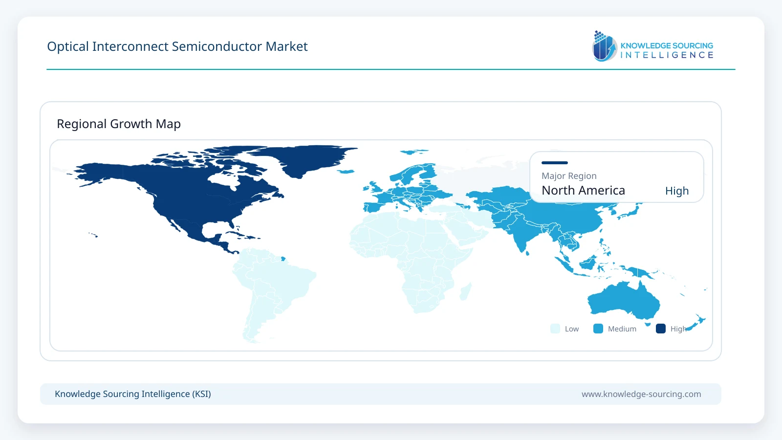
North America is the largest design and premium-demand region for optical interconnect semiconductors because the United States combines hyperscale cloud infrastructure, AI accelerator development, high-radix Ethernet switching and a concentrated photonics semiconductor ecosystem. Broadcom and Marvell supply optical DSP, switching and connectivity silicon used across AI networks, while Intel develops silicon-photonics and optical-compute-interconnect technologies.
Coherent and Lumentum provide compound-semiconductor lasers, modulators, photodiodes and other optical components from large U.S.-based development platforms. Cisco contributes through Acacia coherent and pluggable optics, while a group of specialized companies including Ayar Labs, Lightmatter and Ranovus are developing optical I/O and integrated photonic architectures.
Public investment is reinforcing the region’s position in silicon photonics manufacturing. In July 2026, GlobalFoundries signed a letter of intent with the U.S. Department of Commerce for an expected USD 300 million CHIPS research and development award focused on next-generation silicon photonics, advanced optical materials and packaging. The program targets technologies that support NPO and CPO deployment. This matters commercially because photonics scaling depends on more than transistor design: foundry process control, optical-device uniformity, hybrid bonding, fiber attach and wafer-level test must all improve before highly integrated optical engines can reach large AI volumes.
Demand is also unusually concentrated in North America because hyperscalers and AI infrastructure operators are among the earliest adopters of 1.6T optics, 102.4T switching and scale-up fabrics. Their requirements influence semiconductor roadmaps globally, particularly power per bit, fiber density, link reach and repairability. As a result, North American customers often participate directly in optical architecture definition even when wafer fabrication, package assembly or module manufacturing occurs in Asia.
Asia Pacific remains essential to manufacturing through Taiwan, China, Japan, South Korea and Southeast Asia. The region provides advanced semiconductor fabrication, outsourced assembly and test, optical-module production and high-volume electronics manufacturing. Europe contributes through photonics research, InP and specialty semiconductor capabilities, networking technology and automotive/industrial optical applications, but the highest near-term AI-driven semiconductor design value remains concentrated in the North American ecosystem.
Competitive Landscape
Competition spans digital connectivity silicon, silicon photonics, compound-semiconductor devices and integrated optical engines. Broadcom and Marvell compete across optical DSPs, high-speed SerDes, switch connectivity and increasingly CPO. Marvell also combines optical DSPs with silicon photonics and advanced coherent technologies, while its 2026 Polariton acquisition adds plasmonic modulation expertise. Intel differentiates through a vertically integrated silicon-photonics platform with on-chip lasers and optical compute interconnect development. GlobalFoundries participates as a foundry and platform provider rather than as a merchant transceiver supplier, making manufacturing scale and packaging capability central to its position.
Coherent and Lumentum compete across InP lasers, EMLs, photodiodes, VCSELs and optical subassemblies, giving them strong positions where compound-semiconductor performance is difficult to replace with silicon-only implementations. Cisco/Acacia remains important in coherent optics and DSP architectures. Specialized companies such as Ayar Labs, Lightmatter and Ranovus focus on optical I/O and package-level photonic connectivity, while MACOM and Semtech participate in high-speed analog optical components. Competitive advantage increasingly depends on power per bit, 200G/400G lane performance, optical coupling loss, packaging yield, laser reliability and the ability to integrate photonics with leading-edge electronic silicon.
Major companies and ecosystem participants covered: Broadcom, Marvell Technology, Intel, GlobalFoundries, Coherent, Lumentum, Cisco / Acacia, MACOM Technology Solutions, Semtech, Taiwan Semiconductor Manufacturing Company (TSMC), Ayar Labs, Lightmatter, Ranovus, POET Technologies and NVIDIA.
Recent Developments
September 2026: Marvell announced industry-first 2nm optical demonstrations including 400G-per-lane PAM4, 800G ZR/ZR+ and 1.6T coherent-lite technologies.
September 2026: Coherent demonstrated a 3.2T-class pluggable architecture, 6.4T near-packaged optical engine and VCSEL-based scale-up technologies at ECOC 2026.
July 2026: GlobalFoundries signed a letter of intent for an expected USD 300 million U.S. CHIPS R&D award for silicon photonics, optical materials and advanced packaging.
May 2026: GlobalFoundries introduced the SCALE co-packaged optical-module solution supporting Optical Compute Interconnect Multi-Source Agreement requirements.
April 2026: Marvell acquired Polariton Technologies to add high-speed, low-power plasmonics-based modulation to its optical roadmap.
March 2026: Broadcom showcased a 102.4T Ethernet switch with co-packaged optics and 400G-per-lane optical DSP technology at OFC 2026.
Optical Interconnect Semiconductor Market Scope:
| Report Metric | Details |
|---|---|
| Total Market Size in 2026 | USD 8.40 billion |
| Total Market Size in 2032 | USD 22.70 billion |
| Forecast Unit | USD Billion |
| Growth Rate | 18.0% |
| Study Period | 2021 to 2032 |
| Historical Data | 2021 to 2024 |
| Base Year | 2025 |
| Forecast Period | 2026 – 2032 |
| Segmentation | Semiconductor Function, Material Platform, Interconnect Architecture, Link Speed, Application, Geography |
| Companies |
|
Market Segmentation
By Semiconductor Function
Optical Digital Signal Processors
Silicon Photonics Photonic Integrated Circuits
Lasers and Electro-Absorption Modulated Lasers
VCSELs and Parallel Optical Emitters
Photodiodes, Drivers and Transimpedance Amplifiers
Optical I/O Chiplets and CPO Optical Engines
By Material Platform
Silicon and Silicon-on-Insulator
Indium Phosphide
Gallium Arsenide
Silicon Germanium and Complementary Analog Platforms
Hybrid and Heterogeneous Photonic Integration
By Interconnect Architecture
Pluggable Optics
Linear Pluggable Optics
Near-Packaged Optics
Co-Packaged Optics
Optical Compute I/O and Chiplet Interconnect
By Link Speed
400G and Below
800G
1.6T
3.2T and Above
By Application
AI Scale-Up Networks
AI Scale-Out and Ethernet Fabrics
Data Center Interconnect
Telecom and Carrier Networks
High-Performance Computing and Specialized Systems
By Geography
North America
United States
Canada
Asia Pacific
Taiwan
China
Japan
South Korea
Southeast Asia
Europe
Rest of World
Table of Contents
1. EXECUTIVE SUMMARY
1.1. Market Opportunity and Key Findings
1.2. Optical Interconnect Semiconductor Outlook
1.3. Principal Technology and Revenue Pools
2. MARKET OVERVIEW
2.1. Optical Interconnect Semiconductor Architecture
2.2. Electrical-to-Optical Signal Chain
2.3. Pluggable, Near-Packaged and Co-Packaged Optics
2.4. Optical Input/Output and Compute Interconnect
2.5. Semiconductor Packaging and Fiber-Coupling Requirements
3. MARKET SIZE AND FORECAST, 2026-2032
3.1. Global Market Revenue
3.2. Annual Growth Analysis
3.3. Semiconductor Content per Optical Link
4. MARKET BY SEMICONDUCTOR FUNCTION
4.1. Optical Digital Signal Processors
4.2. Silicon Photonics Photonic Integrated Circuits
4.3. Lasers and Electro-Absorption Modulated Lasers
4.4. VCSELs and Parallel Optical Emitters
4.5. Photodiodes, Drivers and Transimpedance Amplifiers
4.6. Optical I/O Chiplets and CPO Optical Engines
5. MARKET BY MATERIAL PLATFORM
5.1. Silicon and Silicon-on-Insulator
5.2. Indium Phosphide
5.3. Gallium Arsenide
5.4. Silicon Germanium and Complementary Analog Platforms
5.5. Hybrid and Heterogeneous Photonic Integration
6. MARKET BY INTERCONNECT ARCHITECTURE
6.1. Pluggable Optics
6.2. Linear Pluggable Optics
6.3. Near-Packaged Optics
6.4. Co-Packaged Optics
6.5. Optical Compute I/O and Chiplet Interconnect
7. MARKET BY LINK SPEED
7.1. 400G and Below
7.2. 800G
7.3. 1.6T
7.4. 3.2T and Above
8. MARKET BY APPLICATION
8.1. AI Scale-Up Networks
8.2. AI Scale-Out and Ethernet Fabrics
8.3. Data Center Interconnect
8.4. Telecom and Carrier Networks
8.5. High-Performance Computing and Specialized Systems
9. REGIONAL MARKET
9.1. North America
9.1.1. United States
9.1.2. Canada
9.2. Asia Pacific
9.2.1. Taiwan
9.2.2. China
9.2.3. Japan
9.2.4. South Korea
9.2.5. Southeast Asia
9.3. Europe
9.4. Rest of World
10. MARKET DYNAMICS
10.1. Drivers
10.1.1. AI Fabric Bandwidth Density
10.1.2. 1.6T-to-3.2T Optical Transition
10.1.3. Power Constraints in High-Speed Electrical Links
10.1.4. Foundry and Photonic Packaging Scale-Up
10.2. Restraints
10.2.1. Optical Packaging and Fiber-Attach Cost
10.2.2. Laser Reliability and Thermal Management
10.2.3. CPO Serviceability and Repairability
10.2.4. Architecture and Standards Fragmentation
11. COMPETITIVE LANDSCAPE
11.1. Market Structure and Competitive Intensity
11.2. Optical DSP and Connectivity Silicon Positioning
11.3. Silicon Photonics and Foundry Strategies
11.4. InP, VCSEL and Laser Platform Strategies
11.5. CPO and Optical I/O Ecosystem Partnerships
12. COMPANY PROFILES
12.1. Broadcom
12.2. Marvell Technology
12.3. Intel
12.4. GlobalFoundries
12.5. Coherent
12.6. Lumentum
12.7. Cisco / Acacia
12.8. MACOM Technology Solutions
12.9. Semtech
12.10. Taiwan Semiconductor Manufacturing Company
12.11. Ayar Labs
12.12. Lightmatter
12.13. Ranovus
12.14. POET Technologies
12.15. NVIDIA
13. RECENT DEVELOPMENTS
14. APPENDIX
Navigate
Trusted by the world's leading organizations











