
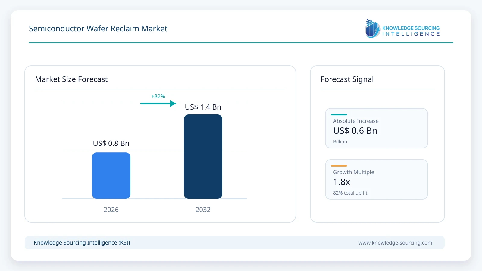
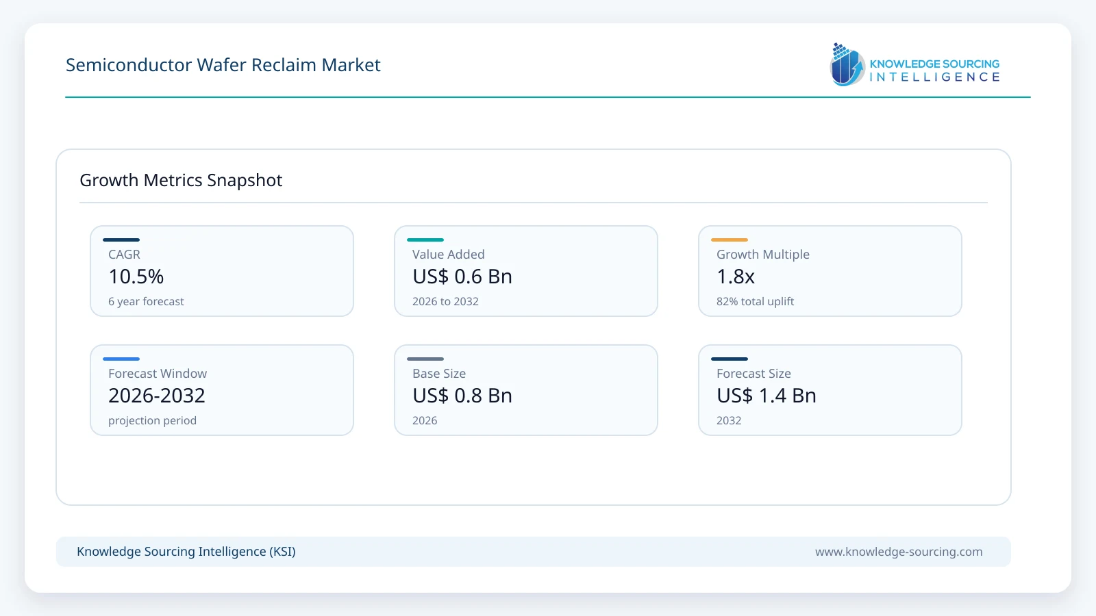
The Semiconductor Wafer Reclaim Market is estimated at USD 0.78 billion in 2026 and is projected to reach USD 1.42 billion by 2032, representing a CAGR of 10.5% during the forecast period.
Highlights:
- 1300 mm reclaim remains the principal growth pool as leading-edge logic, memory and advanced packaging capacity expands.
- 2Advanced nodes increase the number and quality requirements of monitor and dummy wafers used throughout process control.
- 3Copper and non-copper segregation, low particle counts and tighter surface-metal specifications raise qualification barriers.
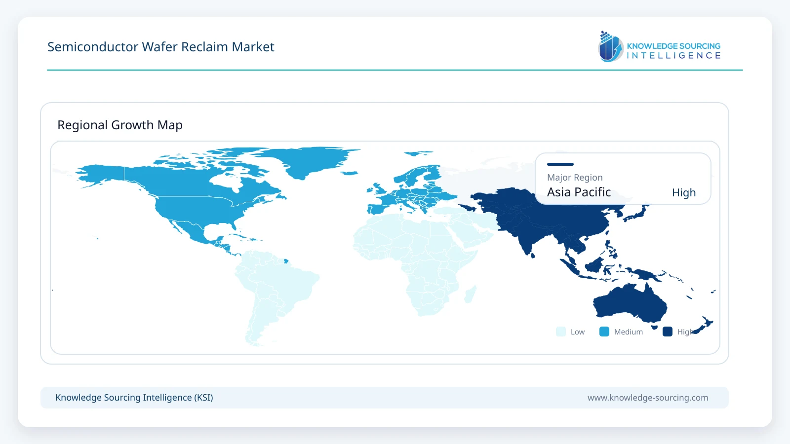
- 4Asia Pacific remains the largest reclaim ecosystem because Taiwan, South Korea and Japan combine high fab density with specialized suppliers.
- 5Local capacity and turnaround time become more important as fabs seek to reduce working capital tied up in circulating monitor wafers.
Market Overview
Reclaimed wafers are primarily created from used monitor, dummy and test wafers rather than rejected production wafers. A typical reclaim flow begins with incoming inspection and sorting, followed by removal of deposited films and surface damage. The wafer may then be ground or lapped, chemically etched, polished, cleaned and inspected before being returned to the customer as a process-support wafer. Pure Wafer distinguishes reclaim from simple recycling: recycling removes films while preserving wafer thickness, whereas reclaim also re-polishes the surface to remove scratches, haze or residual patterns. Each reclaim cycle removes a small amount of silicon, so usable lifetime is ultimately constrained by wafer thickness, edge geometry and customer specifications.
The value proposition is strongest in high-volume fabs because process monitoring consumes a large circulating pool of non-product wafers. Monitor wafers are used to verify deposition thickness, etch behavior, thermal uniformity, contamination and equipment stability. Dummy wafers support chamber conditioning, lot balancing and tool setup. As process sequences become longer and the number of critical control steps increases, the same production capacity can require more monitor-wafer cycles even if final product-wafer starts do not increase proportionally. Reclaim therefore benefits both from new fab construction and from rising process complexity inside existing fabs.
Quality requirements are moving closer to prime-wafer standards for the most demanding applications. KINIK uses ductile-mode grinding to reduce subsurface damage and contamination. Pure Wafer advertises reclaim inspection down to 19 nm and 26 nm defect-count thresholds, while Taiwanese suppliers publish 300 mm particle and metal-contamination specifications that support advanced process monitoring. The commercial market is therefore segmented less by simple wafer diameter alone and increasingly by achievable particle performance, flatness, contamination control, allowable reclaim cycles, turnaround time and customer qualification status.
Market Drivers
Advanced-node fabs consume more process-control wafer cycles
Leading-edge logic and memory manufacturing introduces more deposition, etch, clean, anneal, inspection and metrology steps than mature-node production. Each additional critical step creates opportunities for monitor and dummy wafers to verify chamber condition and process stability before product wafers are exposed. This raises demand for high-grade reclaimed wafers with lower particle counts and tighter surface-metal limits. KINIK is directing its 2026 capacity additions specifically toward high-end reclaim for advanced-node customers, indicating that growth is increasingly concentrated in higher-specification 300 mm products rather than undifferentiated test wafers.
Global 300 mm wafer activity is recovering with AI-related demand
SEMI reported worldwide silicon-wafer shipments of 3,573 million square inches in the second quarter of 2026, up 7.4% year on year and 9.1% sequentially. The organization attributes growth to AI-related demand across advanced logic, memory, power devices and photonics, while broader industrial and automotive markets are also improving. Higher fab utilization expands the number of qualification and monitor cycles, supporting reclaim volumes even though reclaimed wafers are not counted as new wafer shipments in the same way as virgin material.
Wafer cost and sustainability favor repeated substrate reuse
Silicon wafers represent a recurring material cost inside semiconductor manufacturing, especially when fabs use large numbers of non-product wafers for process control. Reclaim reduces purchases of virgin test wafers and keeps high-purity silicon in productive use for multiple cycles. The benefit is both financial and operational: fewer replacement wafers are required, less material is discarded, and fabs can maintain larger controlled inventories of qualified monitor wafers. Sustainability targets therefore reinforce an economic practice that has already been established for decades.
Localized reclaim capacity reduces turnaround time and circulating inventory
Reclaim is a logistics-sensitive service because used wafers must leave the fab, be processed, inspected and returned before they can re-enter the monitor-wafer pool. Long transport cycles force customers to hold more inventory in circulation. This favors reclaim facilities located near major manufacturing clusters in Taiwan, Japan, South Korea, China and the United States. Capacity expansion by KINIK and Scientech in Taiwan is therefore strategically important not only because of absolute volume but also because it shortens the supply loop for major foundries and memory producers.
Restraints and Adoption Challenges
Reclaim economics are constrained by wafer thickness loss, limited usable cycles and increasingly strict process specifications. Some wafers become unsuitable after repeated polishing, edge damage, deep scratches or contamination. Copper-bearing wafers require controlled segregation from non-copper streams to prevent cross-contamination. Advanced fabs also impose long qualification programs because a monitor wafer that carries particles or trace metals can compromise equipment stability and yield. At the same time, low virgin-wafer prices during weaker semiconductor cycles can temporarily narrow the cost advantage of reclaim. These factors favor suppliers with high process yield, strong metrology, local scale and long-standing customer certifications.
Segment Analysis
By Wafer Diameter and Process Grade
300 mm reclaimed wafers represent the central commercial opportunity because advanced logic, DRAM, NAND, high-bandwidth memory and many new fabs operate on 300 mm platforms. Demand is shifting toward lower particle counts, improved total-thickness variation and cleaner copper/non-copper segregation as reclaimed wafers are used closer to critical process modules. The 200 mm segment remains important for analog, power, microcontrollers, MEMS, sensors and specialty devices, where mature fabs often operate at high utilization and place strong value on extending wafer life. Smaller diameters persist in research, compound-semiconductor and specialized manufacturing environments but account for a smaller share of mainstream silicon reclaim activity.
By Application
Monitor and process-control wafers form the most technically demanding application because they are repeatedly inserted into production equipment to verify deposition, etch, cleaning, thermal and contamination performance. Dummy and equipment-conditioning wafers provide a large volume base across furnaces, deposition chambers and other process modules. Test and qualification wafers are used by semiconductor equipment manufacturers, process-development teams and research laboratories. Reclaim suppliers increasingly differentiate these applications by particle specification, surface-metal limits, flatness and traceability rather than treating every reclaimed substrate as interchangeable.
Reclaim Category | Commercial Position | Key Process Requirement | Primary Use |
300 mm high-grade reclaim | Fastest value growth | Low particle count, tight TTV, trace metals control | Advanced logic, memory and high-end process monitoring |
300 mm standard reclaim | Largest volume pool | Reliable film removal, polish and clean | Dummy, monitor and equipment qualification |
200 mm reclaim | Established | Broad film-removal capability and thickness control | Analog, power, MEMS, sensors and mature-node fabs |
Copper-segregated reclaim | Growing specialization | Dedicated Cu/non-Cu flow and contamination control | BEOL and copper-process monitoring |
Specialty / research reclaim | Niche | Custom thickness, resistivity, surface and film specifications | R&D, equipment OEMs and specialty processes |
Market and Technology Indicators
Indicator | 2026 Evidence | Market Implication |
Global silicon-wafer activity | SEMI reported Q2 2026 shipments of 3,573 MSI, up 7.4% year on year. | Higher fab utilization supports more monitor and qualification cycles. |
KINIK capacity expansion | 12-inch reclaim/test/specialty capacity reached 360K wafers/month in Q2 and is targeted at 400K from Q3. | Shows strong demand for high-end 300 mm reclaim in Taiwan. |
Scientech 300 mm expansion | Company targets roughly 250K wafers/month during 2026 with separated Cu and non-Cu processing. | Adds qualified capacity close to leading foundry and DRAM customers. |
Pure Wafer low-particle capability | 100-300 mm reclaim with inspection capability down to 19 nm / 26 nm defect counts. | Raises the usable range of reclaim in tighter process-control applications. |
Precision surface cleaning | Pure Wafer launched PSC methods in 2026 for atomic-level contamination challenges. | Cleaning capability becomes more important as device structures and materials become more sensitive. |
Regional supplier density | Taiwan hosts KINIK, Scientech, Phoenix Silicon and other specialized reclaim providers. | Proximity supports shorter cycle times and lower circulating wafer inventory. |
Regional Opportunity
Asia Pacific
Asia Pacific is the largest market for semiconductor wafer reclaim because it contains the world’s densest concentration of 300 mm foundries, memory fabs, integrated device manufacturers and semiconductor equipment operations. Taiwan is especially important: the island combines TSMC and other fabs with a specialized reclaim supplier base that includes KINIK, Scientech, Phoenix Silicon International, RS Technologies’ Taiwan operations and additional local processors. Capacity additions during 2026 indicate that reclaim demand is tightening around advanced-node requirements rather than simply following mature-node wafer volumes.
Taiwan’s advantage is the proximity between fab customers and reclaim plants. Short transport distances reduce turnaround time and the amount of working capital trapped in wafers moving between the fab and reclaimer. They also make it easier to maintain separate copper and non-copper logistics, respond to specification changes and support rapid qualification. KINIK’s move from 360,000 to 400,000 12-inch wafers per month and Scientech’s 300 mm expansion demonstrate the scale required to serve leading-edge customers. Japan remains strategically important through RS Technologies and Mimasu, while South Korea contributes large captive and merchant demand from memory and logic production.
China and Southeast Asia add growth through new fabs, mature-node capacity, packaging and equipment operations. Although the most demanding reclaim specifications are concentrated around leading-edge clusters, 200 mm and standard 300 mm reclaim remain important for power, analog, microcontroller and industrial semiconductor production. The region therefore supports a layered market ranging from high-grade advanced-node monitor wafers to cost-oriented dummy and test wafers.
North America is smaller in total reclaim volume but strategically important because of new domestic fab investment and local supply-chain resilience. Pure Wafer operates multiple U.S. facilities and positions itself as the largest wafer reclaimer in North America. Europe contributes through specialty semiconductor manufacturing, automotive and power devices, research fabs and equipment qualification, although the local merchant-reclaim supplier base is less concentrated than in East Asia.
Competitive Landscape
Competition is based on qualified capacity, yield, contamination performance, reclaim-cycle capability, turnaround time and proximity to semiconductor fabs. RS Technologies, KINIK, Scientech, Phoenix Silicon International and Mimasu are significant Asia-based participants, while Pure Wafer is a major North American supplier. Customer qualification creates meaningful barriers because reclaim suppliers must demonstrate stable particle counts, flatness, trace metals and wafer identification over repeated production lots.
The market is becoming more technically segmented. Advanced-node customers require lower defect counts, dedicated copper/non-copper processing, better metrology and tighter thickness control. Suppliers that can reclaim wafers with minimal silicon removal can increase the number of useful cycles and improve customer economics. At the same time, local capacity matters because short turnaround reduces the number of wafers that a fab must hold in transit. Scale alone is therefore insufficient unless it is paired with process capability and geographic access to major customers.
Sustainability is an additional differentiator, but the core purchasing decision remains operational. Fabs prioritize predictable quality, fast cycle time and low contamination because monitor-wafer failures can disrupt production equipment. Reclaim providers are consequently investing in automated tracking, advanced inspection, precision cleaning and higher-capacity 300 mm lines rather than competing only on unit processing price.
Major companies and ecosystem participants covered: RS Technologies, KINIK Company, Scientech Corporation, Phoenix Silicon International, Pure Wafer, Mimasu Semiconductor Industry, Hamada Heavy Industries, TOPCO Scientific, Scientia Technology, GlobalWafers ecosystem partners, regional wafer-processing specialists and semiconductor equipment qualification providers.
Recent Developments
May 2026: KINIK reported 12-inch reclaim/test/specialty-wafer capacity of 360,000 wafers per month from the second quarter, with a further expansion to 400,000 wafers per month from the third quarter.
2026: KINIK stated that newly added reclaim capacity is being directed toward high-end wafers for advanced-node customers to improve product mix and margins.
2026: Scientech outlined expansion of its 300 mm reclaim operation toward approximately 250,000 wafers per month with separated copper and non-copper process capability.
June 2026: Pure Wafer announced Precision Surface Cleaning methods aimed at atomic-level contamination removal for advanced semiconductor, AI and quantum-sensing applications.
July 2026: SEMI reported second-quarter global silicon-wafer shipments of 3,573 million square inches, up 7.4% year on year, supported by AI-related semiconductor demand.
Semiconductor Wafer Reclaim Market Scope:
| Report Metric | Details |
|---|---|
| Total Market Size in 2026 | USD 0.78 billion |
| Total Market Size in 2032 | USD 1.42 billion |
| Forecast Unit | USD Billion |
| Growth Rate | 10.5% |
| Study Period | 2021 to 2032 |
| Historical Data | 2021 to 2024 |
| Base Year | 2025 |
| Forecast Period | 2026 – 2032 |
| Segmentation | Wafer Diameter, Reclaim Grade, Application, Customer Type, Geography |
| Companies |
|
Market Segmentation
By Wafer Diameter
300 mm Reclaimed Wafers
200 mm Reclaimed Wafers
150 mm and Smaller Wafers
By Reclaim Grade
Advanced Low-Particle Reclaim
Standard Monitor-Wafer Reclaim
Dummy and Equipment-Conditioning Wafers
Copper-Segregated Reclaim
Specialty and Custom Reclaim
By Application
Process Monitoring and Metrology
Equipment Qualification and Chamber Conditioning
Process Development and R&D
Semiconductor Equipment OEMs
Specialty Manufacturing
By Customer Type
Foundries
Integrated Device Manufacturers
Memory Manufacturers
Semiconductor Equipment Companies
Research and Specialty Fabs
By Geography
Asia Pacific
Taiwan
Japan
South Korea
China
Southeast Asia
North America
Europe
Rest of World
Table of Contents
1. EXECUTIVE SUMMARY
1.1. Market Opportunity and Key Findings
1.2. Reclaimed Wafer Demand Outlook
1.3. Principal Revenue Pools
2. MARKET OVERVIEW
2.1. Wafer Reclaim Process Flow
2.2. Monitor, Dummy and Test Wafer Lifecycle
2.3. Reclaim versus Recycling
2.4. Particle, Flatness and Metal-Contamination Requirements
2.5. Reclaim Cycle Limits and Wafer Thickness
3. MARKET SIZE AND FORECAST, 2026-2032
3.1. Global Market Revenue
3.2. Annual Growth Analysis
3.3. Reclaim Volume and Value Drivers
4. MARKET BY WAFER DIAMETER
4.1. 300 mm Reclaimed Wafers
4.2. 200 mm Reclaimed Wafers
4.3. 150 mm and Smaller Wafers
5. MARKET BY RECLAIM GRADE
5.1. Advanced Low-Particle Reclaim
5.2. Standard Monitor-Wafer Reclaim
5.3. Dummy and Equipment-Conditioning Wafers
5.4. Copper-Segregated Reclaim
5.5. Specialty and Custom Reclaim
6. MARKET BY APPLICATION
6.1. Process Monitoring and Metrology
6.2. Equipment Qualification and Chamber Conditioning
6.3. Process Development and R&D
6.4. Semiconductor Equipment OEMs
6.5. Specialty Manufacturing
7. MARKET BY CUSTOMER TYPE
7.1. Foundries
7.2. Integrated Device Manufacturers
7.3. Memory Manufacturers
7.4. Semiconductor Equipment Companies
7.5. Research and Specialty Fabs
8. REGIONAL MARKET
8.1. Asia Pacific
8.1.1. Taiwan
8.1.2. Japan
8.1.3. South Korea
8.1.4. China
8.1.5. Southeast Asia
8.2. North America
8.3. Europe
8.4. Rest of World
9. MARKET DYNAMICS
9.1. Drivers
9.1.1. Advanced-Node Monitor-Wafer Intensity
9.1.2. Growth in 300 mm Fab Utilization
9.1.3. Wafer Cost and Sustainability
9.1.4. Local Turnaround and Inventory Economics
9.2. Restraints
9.2.1. Limited Reclaim Cycles and Thickness Loss
9.2.2. Copper and Metal-Contamination Risk
9.2.3. Customer Qualification Requirements
9.2.4. Virgin Test-Wafer Pricing Cycles
10. COMPETITIVE LANDSCAPE
10.1. Market Structure and Competitive Intensity
10.2. 300 mm High-Grade Reclaim Positioning
10.3. Regional Capacity and Fab Proximity
10.4. Inspection, Cleaning and Traceability Capability
10.5. Capacity Expansion Strategies
11. COMPANY PROFILES
12. RECENT DEVELOPMENTS
13. APPENDIX
Navigate
Trusted by the world's leading organizations











