
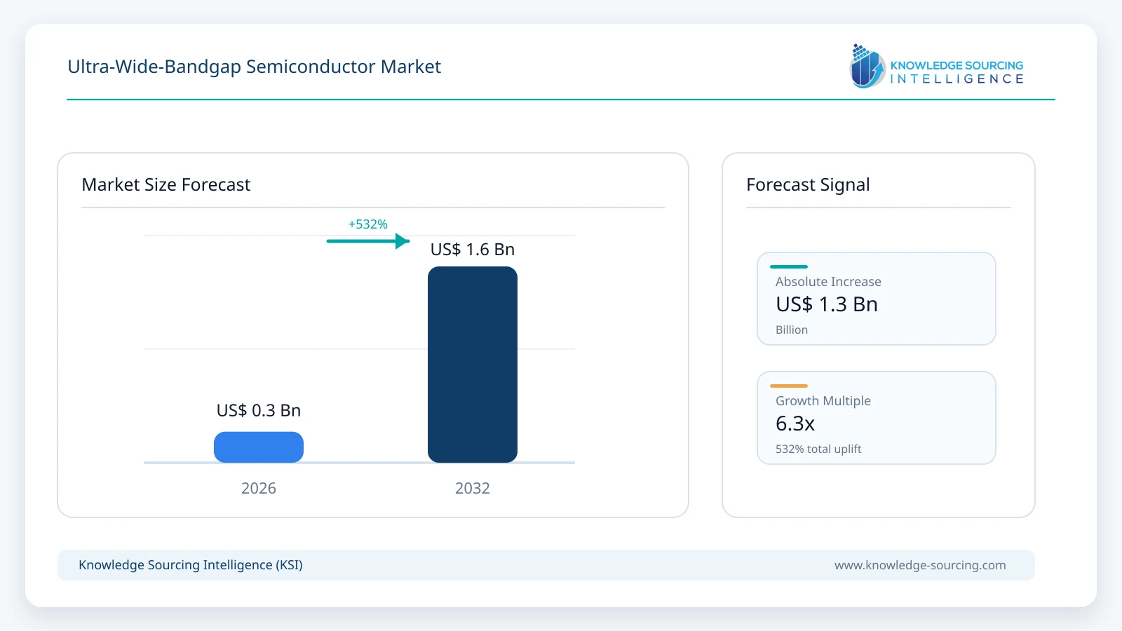
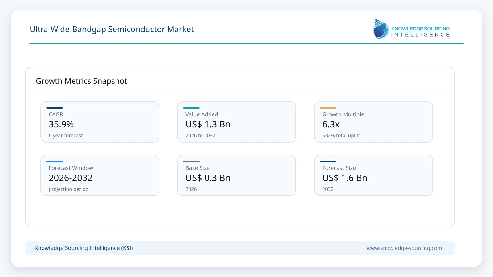
The Ultra-Wide-Bandgap Semiconductor Market is estimated at USD 0.25 billion in 2026 and is projected to reach USD 1.58 billion by 2032, representing a CAGR of 35.9% during the forecast period.
Key Highlights
· Gallium oxide represents the largest commercial UWBG semiconductor platform in 2026.
· Aluminum nitride has the strongest near-term large-wafer pathway through 76 mm and 100 mm substrates.
· Diamond semiconductor devices are progressing from material qualification into early RF and power products.
· Power electronics is the largest long-term application, while RF and defense provide earlier premium-volume demand.
· Commercial growth accelerates after 2028 as larger wafers and production-qualified device processes become available.
Market Overview
UWBG semiconductors generally have bandgaps materially larger than GaN and silicon carbide and can sustain very high electric fields before breakdown. DARPA's UWBGS program identifies diamond, cubic boron nitride and aluminum nitride as priority materials because of their potential for high-voltage switching, high-power radio-frequency electronics, extreme-environment electronics and deep-ultraviolet devices. Gallium oxide is also widely treated as a leading UWBG power-semiconductor platform because of its approximately 4.8 to 4.9 eV bandgap and the ability to grow bulk crystals from a melt.
The commercial maturity of each material differs substantially. Gallium oxide has the clearest power-device manufacturing roadmap: substrates and epitaxial wafers are already sold, 100 mm products are available to developers, and 150 mm samples entered the market in 2026. Aluminum nitride has a more established substrate business because it supports both Al-rich nitride optoelectronics and future power/RF devices. Diamond has strong material performance and emerging commercial devices, but large-area semiconductor-grade wafers, reproducible doping and contact resistance remain constraints. Cubic boron nitride is still predominantly in foundational materials development.
The market therefore should not be viewed as a direct substitute for today's SiC or GaN device industry. The near-term revenue base comes from high-value substrates, epiwafers, development devices and defense or research programs. Larger commercial power-device revenue emerges later in the forecast as wafers reach production-compatible diameters and device makers demonstrate stable yields, reliable contacts and manufacturable vertical device structures.
Market Drivers
High-voltage power electronics requires materials beyond current WBG limits
Electric grids, industrial power systems, aerospace platforms and future megawatt-class converters increasingly require high blocking voltage with lower conduction and switching losses. Gallium oxide, AlN and diamond offer theoretical critical electric fields above mainstream GaN and SiC. A 2026 Nature Communications demonstration of a gallium oxide module switching 1000 V and 1000 A in pulsed operation shows that UWBG devices can begin addressing power levels that previously remained outside practical demonstrations. Continued progress in packaging and thermal design can therefore translate material advantages into system-level power density.
Larger wafers are moving UWBG materials toward manufacturable platforms
Wafer diameter is one of the clearest indicators of commercialization because larger substrates allow UWBG materials to enter existing semiconductor tool sets and reduce device cost per unit area. Novel Crystal Technology began 150 mm gallium oxide sample shipments in 2026 and targets full-scale 150 mm epiwafer production in 2029. HexaTech released 76.2 mm AlN substrates, while Crystal IS has demonstrated serial production of 100 mm single-crystal AlN with high usable area. Orbray's 30 mm square (111) diamond substrate similarly addresses the scaling barrier that has historically restricted diamond device manufacturing.
Defense and extreme-environment electronics create early premium markets
UWBG materials can tolerate combinations of voltage, temperature, radiation and RF power that are difficult for conventional semiconductor platforms. DARPA is funding substrate, device-layer and contact development across AlN, diamond and cubic boron nitride, while Raytheon and Northrop Grumman are participating in device programs. Advent Diamond and Northrop Grumman demonstrated a diamond-based solid-state limiter handling more than 100 W in 2026. These applications provide high-value early markets even before automotive or grid-scale power devices reach mass production.
Materials investment is expanding beyond isolated research programs
Commercial suppliers are building broader ecosystems around UWBG materials. Novel Crystal Technology has attracted strategic investment from companies including Mitsubishi Electric, ROHM, AGC and Tamura, while Kyma Technologies is collaborating on large-area gallium oxide epiwafers. Stanley Electric owns HexaTech, and Asahi Kasei is concentrating Crystal IS resources on AlN substrates. In diamond, Element Six, Orbray, Coherent and Advent Diamond are advancing different substrate and device approaches. This diversification increases the probability that more than one UWBG material reaches commercially sustainable applications.
Restraints and Adoption Challenges
UWBG semiconductors remain technically immature relative to silicon carbide and GaN. Gallium oxide has low thermal conductivity and lacks a practical native p-type device architecture, complicating high-power thermal management and bipolar structures. Diamond offers exceptional thermal conductivity but still faces challenges in large-area substrates, doping and low-resistance contacts. Aluminum nitride combines high thermal conductivity with a very wide bandgap, yet controlled doping and device-layer growth remain difficult. Cubic boron nitride is further from volume production. The absence of established foundry processes, qualified packaging, long-term reliability data and standardized supply chains means device makers must fund significant application engineering before volume deployment.
Segment Analysis
By Material
Gallium oxide represents the largest revenue contribution in 2026 because commercial substrate and epiwafer suppliers already serve power-device development programs and the material has a relatively clear transition path toward 150 mm manufacturing. Its ability to use melt-grown bulk crystals can provide a cost advantage if defect control and thermal limitations are managed successfully.
Diamond semiconductors are expected to record the fastest growth through 2032 from a smaller commercial base. The combination of high breakdown strength, carrier mobility and exceptional thermal conductivity is attractive for RF, power and extreme-environment devices. Aluminum nitride remains a substantial substrate market with strong long-term prospects in high-voltage and high-frequency electronics. Cubic boron nitride and other emerging UWBG materials contribute limited revenue through 2032 but remain important technology options.
Material / Platform | Revenue Contribution | Growth Direction | Primary Semiconductor Application |
Gallium oxide (Ga2O3) | Largest | Very strong | High-voltage power devices, diodes, transistors and pulsed-power switching |
Aluminum nitride (AlN) | High | Very strong | Power/RF substrates, Al-rich nitride devices and deep-UV electronics |
Diamond semiconductor | Growing | Fastest | High-power RF, power switching, radiation-hard and extreme-temperature electronics |
High-Al AlGaN / AlN heterostructures | Emerging | Very fast | High-field RF and power devices |
Cubic boron nitride and other UWBG materials | Small | Early stage | Extreme-field electronics and advanced research devices |
UWBG epiwafers and device layers | Core enabling category | Very strong | Production-quality active layers on large-area substrates |
Market and Technology Indicators
Indicator | Revenue Contribution | Market Impact |
150 mm gallium oxide samples | Novel Crystal Technology began 150 mm substrate sample shipments in March 2026 and targets 150 mm epiwafer mass production in 2029. | Moves Ga2O3 toward compatibility with production-scale power-semiconductor manufacturing. |
Lower-cost Ga2O3 crystal growth | Novel Crystal Technology developed a crucible-light DG method targeting roughly one-tenth conventional substrate cost. | Addresses one of the main economic barriers to gallium oxide scaling. |
3-inch AlN production release | HexaTech launched 76.2 mm single-crystal AlN substrates in February 2026. | Creates a bridge toward 100 mm commercial AlN manufacturing. |
100 mm AlN focus | Crystal IS shifted resources toward AlN substrates after achieving 100 mm material suitable for semiconductor evaluation. | Strengthens a second commercial UWBG substrate supply path. |
Large-area diamond progress | Orbray demonstrated a 30 mm square twin-free (111) single-crystal diamond substrate in 2026. | Reduces a major scaling constraint for diamond power and quantum devices. |
Megawatt-class Ga2O3 module | A 2026 Nature Communications study demonstrated 1000 V, 1000 A pulsed switching in a multi-die gallium oxide module. | Shows UWBG devices moving from discrete demonstrations toward packaged high-power systems. |
Regional Opportunity
Asia Pacific
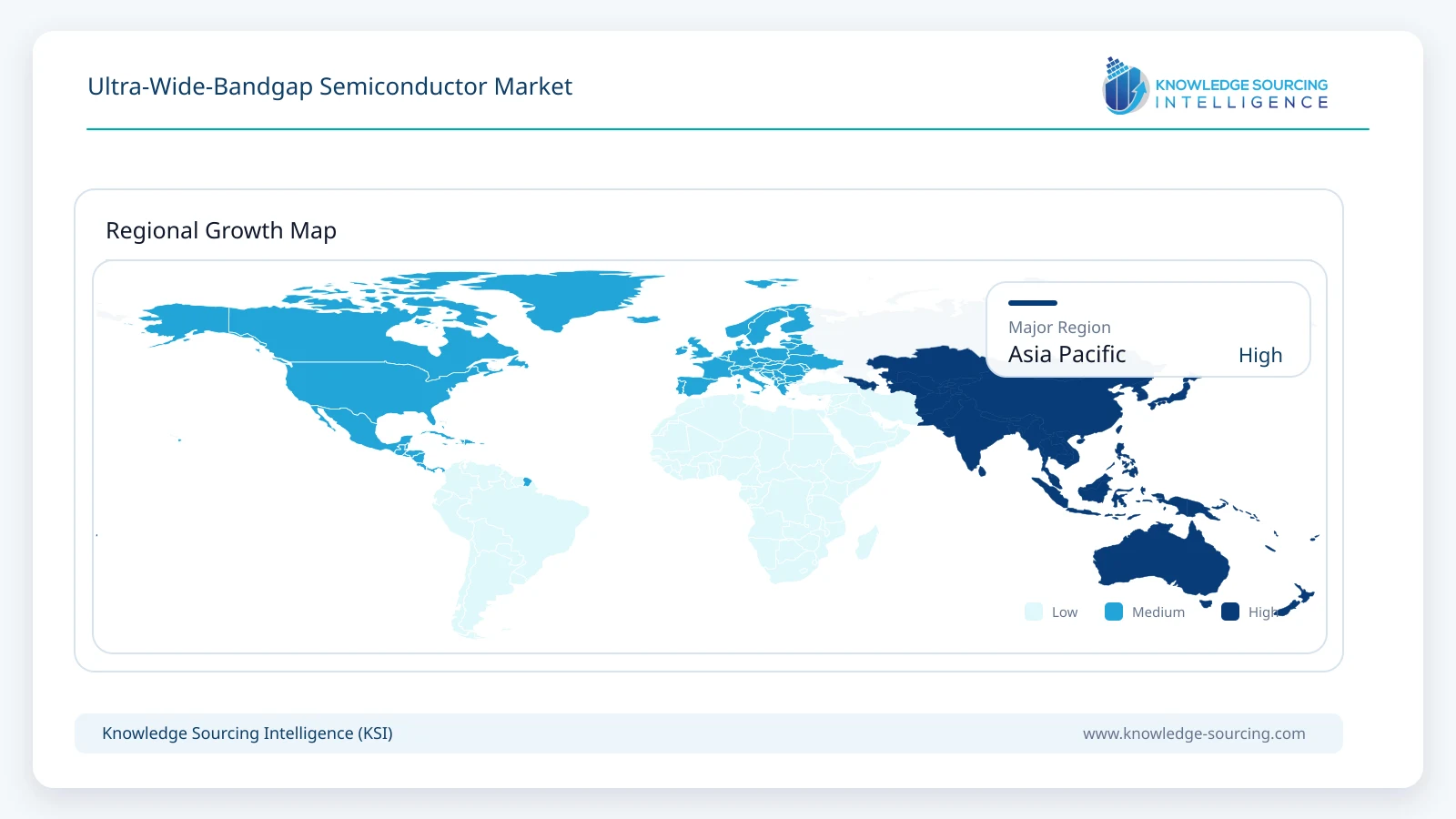
Asia Pacific is the largest commercial region for UWBG semiconductors in 2026 because Japan contains several of the most advanced gallium oxide, aluminum nitride and diamond-material programs alongside established power-semiconductor and electronics manufacturing. Novel Crystal Technology is the leading commercial gallium oxide substrate and epiwafer supplier, FLOSFIA is advancing alpha-gallium-oxide power devices, Orbray is scaling single-crystal diamond substrates, and Asahi Kasei is concentrating Crystal IS on AlN substrate development. Strategic investors including Mitsubishi Electric, ROHM, AGC and Tamura connect emerging materials with established semiconductor and industrial markets.
Japan's gallium oxide ecosystem has the most visible transition from research to industrial planning. Novel Crystal Technology is shipping 150 mm samples in 2026 and targets 150 mm epiwafer mass production in 2029, while its new crystal-growth method is intended to reduce substrate cost significantly. FLOSFIA is pursuing a different alpha-phase gallium oxide platform using mist deposition and continues commercialization work around power devices. The coexistence of bulk beta-gallium-oxide and epitaxial alpha-gallium-oxide approaches provides the region with multiple technical paths.
Diamond commercialization is also centered strongly in Japan. Orbray has expanded its heteroepitaxial substrate roadmap from 20 mm to 30 mm square (111) material and is developing doped substrates for device applications. Collaboration with MIRISE Technologies links diamond development to automotive power electronics. Japanese materials expertise also extends into high-purity processing, polishing and packaging, which are critical because diamond performance depends heavily on surface preparation and low-defect interfaces.
North America remains a major development and early-adoption market through DARPA's UWBGS program, HexaTech, Crystal IS, Kyma Technologies, Advent Diamond, Coherent, Raytheon and Northrop Grumman. The region is particularly strong in defense, RF, extreme-environment and semiconductor-material programs. Europe contributes through Element Six and advanced materials research, while other regions remain smaller and are primarily involved through university and government-funded semiconductor development.
Competitive Landscape
The competitive landscape is fragmented because each UWBG material has a different manufacturing route and commercial maturity. Novel Crystal Technology and FLOSFIA represent distinct gallium oxide approaches, with NCT centered on beta-gallium-oxide substrates and epiwafers and FLOSFIA focused on alpha-gallium-oxide device technology. Kyma Technologies adds epitaxial capability and a U.S. commercialization route for Ga2O3. HexaTech and Crystal IS are the most visible commercial AlN substrate suppliers, with current programs aimed at larger diameters and electronic-device quality.
Diamond has a broader set of participants. Orbray and Element Six focus heavily on large-area single-crystal material, Coherent supplies electronic-grade CVD diamond and is participating in U.S. ultrawide-bandgap commercialization programs, while Advent Diamond is developing and selling all-diamond semiconductor components. Raytheon and Northrop Grumman participate in defense-oriented UWBG device development and validation. Established semiconductor and materials companies including Mitsubishi Electric, ROHM, AGC and Tamura support commercialization through investment, device expertise and potential downstream adoption.
Competition is based on substrate diameter, defect density, doping control, epitaxial quality, contact resistance, thermal performance and the ability to demonstrate reliable devices rather than on wafer price alone. Because the industry remains early, strategic partnerships between material suppliers, device companies and defense or industrial users are more important than conventional high-volume channel scale. Suppliers that reach 100 mm to 150 mm manufacturing while maintaining defect and electrical uniformity will be best positioned for commercial adoption after 2028.
Major companies and ecosystem participants covered: Novel Crystal Technology, FLOSFIA, Kyma Technologies, HexaTech / Stanley Electric, Crystal IS / Asahi Kasei, Orbray, Element Six, Coherent, Advent Diamond, RTX / Raytheon, Northrop Grumman, Mitsubishi Electric, ROHM, AGC and Tamura Corporation.
Recent Developments
· May 2026: Advent Diamond and Northrop Grumman demonstrated a diamond-based solid-state limiter handling more than 100 W of RF power.
· March 2026: A Nature Communications study demonstrated a flip-chip gallium oxide module capable of 1000 V and 1000 A pulsed switching.
· March 2026: Orbray published results for a 30 mm square twin-free (111) single-crystal diamond substrate for power and quantum devices.
· March 2026: Asahi Kasei announced that Crystal IS would discontinue UVC LED device production and focus resources on aluminum nitride substrates for RF and power semiconductors.
· February 2026: Novel Crystal Technology announced 150 mm beta-gallium-oxide substrate sample shipments ahead of targeted 2029 mass production.
· February 2026: HexaTech released a 3-inch single-crystal AlN substrate product for commercial-scale AlN-based technology development.
· January 2026: Novel Crystal Technology announced a new gallium-oxide crystal-growth method designed to reduce substrate production cost to about one-tenth of the conventional approach.
Ultra-Wide-Bandgap Semiconductor Market Scope:
| Report Metric | Details |
|---|---|
| Total Market Size in 2026 | USD 0.25 billion |
| Total Market Size in 2032 | USD 1.58 billion |
| Forecast Unit | USD Billion |
| Growth Rate | 35.9% |
| Study Period | 2021 to 2032 |
| Historical Data | 2021 to 2024 |
| Base Year | 2025 |
| Forecast Period | 2026 – 2032 |
| Segmentation | Enablement Layer, UCIe Generation, Package Type, Application, Customer Type, Geography |
| Companies |
|
Market Segmentation
By Enablement Layer
UCIe Controller and Protocol IP
UCIe PHY IP
Verification IP
Design, Package and Signal-Integrity Software
Compliance and Interoperability Test Systems
Integration, Bring-Up and Engineering Services
By UCIe Generation
UCIe 1.x Implementations
UCIe 2.0 and 3D Packaging
UCIe 3.0 48G and 64G Implementations
Future Specification Evolution
By Package Type
Standard Package UCIe
Advanced Package UCIe
2.5D Interposer and Bridge Packages
3D and Hybrid-Bonded Multi-Die Systems
By Application
AI Accelerators and GPUs
High-Performance Computing and Server CPUs
Data-Center Networking and Custom Cloud Silicon
Client and Edge Computing
Automotive Compute
Optical, Memory and Specialized Chiplets
By Customer Type
Fabless Semiconductor Companies
Integrated Device Manufacturers
Cloud and Hyperscale Silicon Developers
Foundries and Advanced Packaging Providers
Automotive and Industrial Semiconductor Companies
IP, EDA and Design-Service Providers
By Geography
North America
United States
Canada
Asia Pacific
Taiwan
South Korea
Japan
China and Southeast Asia
Europe
Rest of World
Table of Contents
1. EXECUTIVE SUMMARY
1.1. Market Opportunity and Key Findings
1.2. UWBG Commercialization Outlook
1.3. Principal Revenue Pools
2. MARKET OVERVIEW
2.1. Ultra-Wide-Bandgap Material Landscape
2.2. Substrate, Epitaxy and Device Maturity
2.3. Power and RF Device Requirements
2.4. Wafer Scaling and Manufacturing Readiness
2.5. UWBG versus SiC and GaN
3. MARKET SIZE AND FORECAST, 2026-2032
3.1. Global Market Revenue
3.2. Annual Growth Analysis
3.3. Materials, Wafers and Device Revenue
4. MARKET BY MATERIAL
4.1. Gallium Oxide
4.2. Aluminum Nitride
4.3. Diamond Semiconductor
4.4. High-Aluminum AlGaN / AlN Heterostructures
4.5. Cubic Boron Nitride and Other UWBG Materials
5. MARKET BY PRODUCT LAYER
5.1. Bulk Substrates and Wafers
5.2. Epitaxial Wafers and Device Layers
5.3. Discrete Power and RF Devices
5.4. Packaged Devices and Modules
5.5. Development and Foundry Services
6. MARKET BY APPLICATION
6.1. High-Voltage Power Conversion
6.2. Pulsed Power and Grid Protection
6.3. High-Power RF and Defense Electronics
6.4. Aerospace and Extreme-Environment Electronics
6.5. Deep-Ultraviolet Optoelectronics
6.6. Quantum and Radiation-Sensing Devices
7. MARKET BY COMMERCIALIZATION STAGE
7.1. Research and Development
7.2. Engineering Samples and Pilot Production
7.3. Early Commercial Devices
7.4. Volume Manufacturing Roadmap
8. MARKET BY END USER
8.1. Power Electronics and Grid Infrastructure
8.2. Defense and Aerospace
8.3. Semiconductor and Electronics Manufacturers
8.4. Automotive and Transportation
8.5. Research, Quantum and Scientific Instrumentation
9. REGIONAL MARKET
9.1. Asia Pacific
9.1.1. Japan
9.1.2. China
9.1.3. South Korea
9.1.4. Rest of Asia Pacific
9.2. North America
9.3. Europe
9.4. Rest of World
10. MARKET DYNAMICS
10.1. Drivers
10.1.1. High-Voltage Power Electronics beyond WBG Limits
10.1.2. Larger UWBG Wafer Availability
10.1.3. Defense and Extreme-Environment Demand
10.1.4. Expansion of Commercial Materials Ecosystems
10.2. Restraints
10.2.1. Doping, Contacts and Device-Architecture Challenges
10.2.2. Thermal Constraints in Gallium Oxide
10.2.3. Large-Area Diamond Manufacturing
10.2.4. Immature Foundry, Packaging and Reliability Ecosystems
11. COMPETITIVE LANDSCAPE
11.1. Market Structure and Competitive Intensity
11.2. Gallium Oxide Substrate and Device Positioning
11.3. Aluminum Nitride Substrate Strategies
11.4. Diamond Semiconductor Commercialization
11.5. Strategic Investment and Defense Ecosystem Partnerships
12. COMPANY PROFILES
12.1. Novel Crystal Technology
12.2. FLOSFIA
12.3. Kyma Technologies
12.4. HexaTech / Stanley Electric
12.5. Crystal IS / Asahi Kasei
12.6. Orbray
12.7. Element Six
12.8. Coherent
12.9. Advent Diamond
12.10. RTX / Raytheon
12.11. Northrop Grumman
12.12. Mitsubishi Electric
12.13. ROHM
12.14. AGC
12.15. Tamura Corporation
13. RECENT DEVELOPMENTS
14. APPENDIX
Navigate
Trusted by the world's leading organizations











