
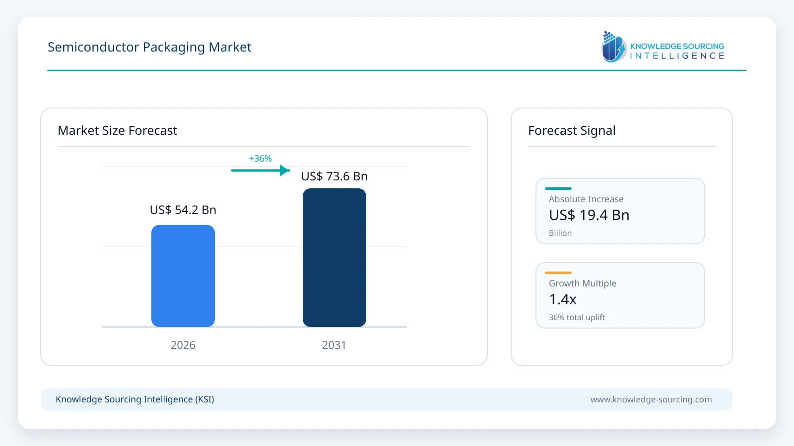
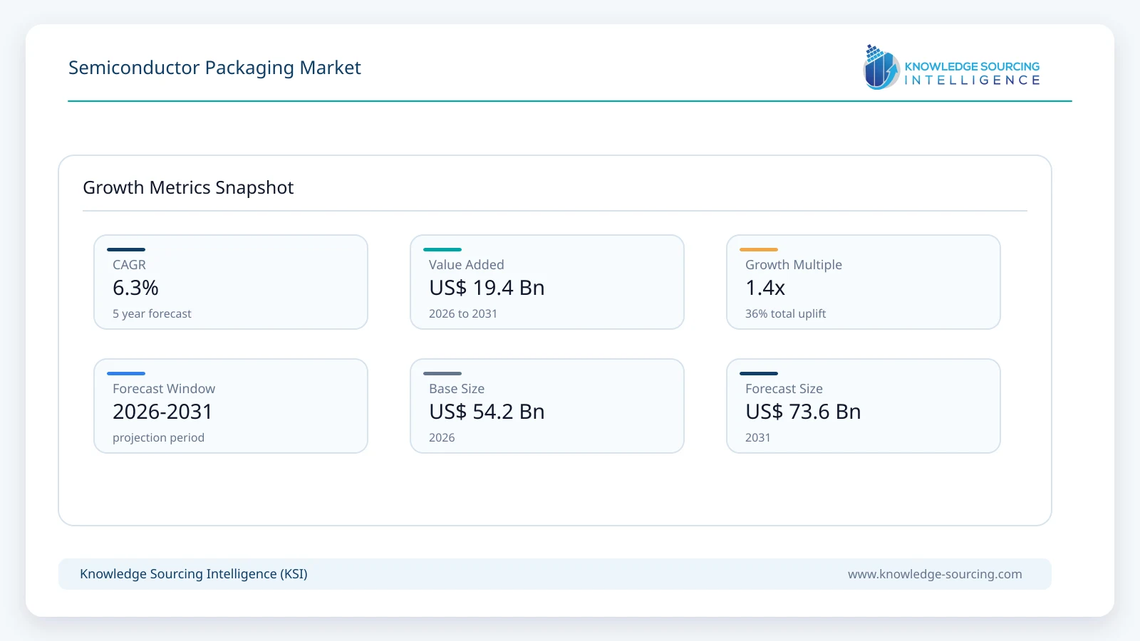
The Semiconductor Packaging Market is projected to expand at a CAGR of 6.3%, reaching USD 73.6 billion in 2031 from USD 54.2 billion in 2026.
Highlights:
- 1Advanced packaging accounts for approximately 74% of global semiconductor packaging value in 2026.
- 2Organic-substrate packages are projected to grow at approximately 6.6% annually through 2031.
- 3Consumer electronics generate about USD 16.3 billion of semiconductor packaging value in 2026.
- 4Asia Pacific represents approximately 66% of global semiconductor packaging revenue in 2026.
- 5AI accelerators are increasing demand for chiplets, high-bandwidth memory and large multi-die packages.
- 6Panel-level packaging is moving toward commercial production for larger AI and high-performance packages.
Semiconductor packaging provides the physical interface between a fabricated die and the electronic system in which it operates. A package protects the die, routes electrical signals, supplies power, removes heat and provides the mechanical form needed for board assembly. Traditional wire-bonded packages remain important for analog, power, microcontroller and cost-sensitive devices. Advanced packages place more of the system integration inside the package through fine-pitch interconnects, redistribution layers, silicon bridges, interposers, through-silicon vias and stacked dies.
The distinction between conventional and advanced packaging is becoming more important as package architecture contributes directly to computing performance. High-performance processors increasingly combine logic dies, high-bandwidth memory and specialized chiplets in a single package. Foundries and integrated device manufacturers are therefore competing more directly with outsourced semiconductor assembly and test companies in selected advanced packaging platforms. At the same time, large OSAT suppliers retain an important role in high-volume mobile, automotive, memory and communications packaging.
Market Trends
AI is shifting package design toward chiplets, high-bandwidth memory and larger integration areas
Advanced AI systems require more memory bandwidth and more compute dies than can be integrated efficiently on a single monolithic chip. This is increasing adoption of 2.5D and 3D integration, silicon bridges and high-density redistribution layers. Intel highlighted its Foveros stacking and Embedded Multi-die Interconnect Bridge technologies in July 2026 as core tools for scaling multi-chip AI packages beyond the reticle limit. TSMC continues to expand CoWoS, InFO and SoIC platforms, while Samsung is developing larger 2.xD package formats for AI and high-performance computing.
Panel-level packaging is moving from development toward higher-volume manufacturing
Larger AI packages reduce the efficiency of round-wafer processing because more usable area is lost at the wafer edge. Panel-level packaging uses a square or rectangular format that can improve material utilization for large packages. ASE announced an automated 310 mm by 310 mm panel-level packaging line in May 2026 for FOCoS and FOCoS-Bridge platforms. The company expects the line to enter production during the first half of 2027. Samsung is also developing panel-level approaches for larger interposers and multi-HBM integration.
Packaging capacity is becoming part of semiconductor supply-chain localization
Governments and customers increasingly want advanced packaging capacity located closer to new wafer-fabrication investments. Amkor expanded its planned Arizona advanced packaging and test campus to approximately USD 12 billion in September 2026. The company also entered a ten-year collaboration framework with TSMC in June 2026 to support advanced packaging and testing in Arizona. These investments reflect the growing strategic role of the back end in AI, automotive and high-performance semiconductor supply chains.
Market Drivers
AI and high-performance computing increase the value created at the package level
Process-node scaling alone is no longer sufficient to deliver the performance required by large AI systems. Packaging allows designers to combine leading-edge logic, memory and specialized dies without manufacturing every function on the same process node. This improves flexibility and can reduce the cost of very large system designs. The resulting demand is supporting investment in 2.5D integration, hybrid bonding, advanced redistribution layers and thermal-management solutions.
Automotive electronics broaden demand across both advanced and mature packaging technologies
Vehicles use semiconductors across powertrain control, infotainment, connectivity, driver assistance, battery management and safety systems. Many automotive devices continue to use mature package formats because long qualification cycles and reliability matter more than maximum integration density. At the same time, advanced driver-assistance and centralized computing platforms require higher-performance processors and memory. The automotive market therefore supports demand across wire-bonded, flip-chip and system-in-package technologies.
Higher semiconductor content in connected devices sustains volume packaging demand
Smartphones, wearables, communications equipment and industrial connected devices require multiple packaged semiconductor components. Miniaturization pushes designers toward smaller footprints and higher integration, while cost-sensitive products continue to rely on high-volume standard packages. This creates a broad demand base for OSAT providers and integrated manufacturers. The combination of mature volume packaging and faster-growing advanced formats supports a more balanced market than AI packaging alone.
Market Restraint
Advanced packaging requires high capital intensity and tighter process control
Complex packages require expensive equipment, cleanroom space, precision bonding and additional inspection steps. Yield loss can become costly because multiple high-value dies and memory stacks may be integrated in the same package. Thermal expansion, warpage and interconnect reliability become more difficult as package size increases. Suppliers must therefore invest heavily in process control, metrology and design co-optimization before new technologies reach high-volume manufacturing.
Segment Analysis
By Packaging Type - Advanced Packaging
Advanced packaging is the largest packaging-type segment because high-value processors, memory devices and system-in-package products increasingly use flip-chip, wafer-level, fan-out, 2.5D or 3D integration. The segment is projected to reach approximately USD 55.9 billion by 2031. Growth is being led by AI accelerators, high-bandwidth memory, premium mobile devices and high-performance networking. Conventional packaging remains important for analog, power, microcontroller and other mature-node devices.
By Primary Package Platform - Organic Substrate
Organic substrates form the largest package-platform segment because ball-grid-array, flip-chip and many multi-die packages rely on laminated substrates for signal routing and mechanical support. The segment is estimated at approximately USD 19.8 billion in 2026. Demand is supported by computing, communications and automotive applications. More complex packages require finer routing, stronger dimensional control and improved thermal performance, which increases technical requirements for high-end substrate suppliers.
By End User - Consumer Electronics
Consumer electronics remain the largest end-user group because smartphones, personal computers, wearables, televisions and connected devices contain large numbers of packaged semiconductors. The segment is projected to grow at approximately 5.2% annually through 2031. Mobile devices support wafer-level, flip-chip and system-in-package demand, while personal computing increasingly uses more advanced processor and memory packaging. The segment grows more slowly than AI infrastructure but remains the largest volume base.
By Geography - Asia Pacific
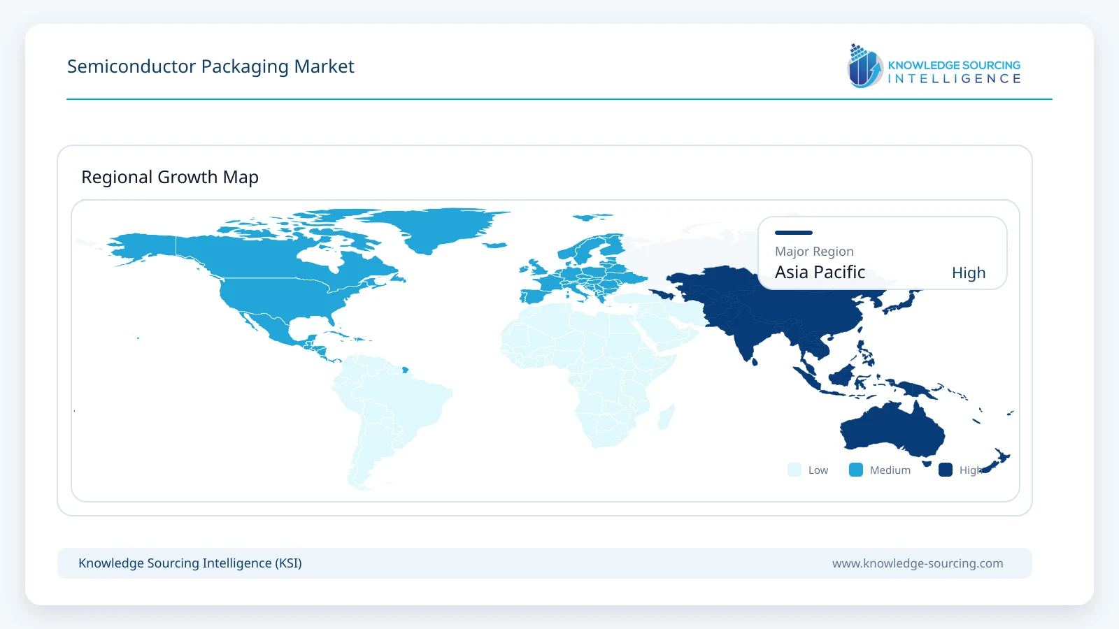
Asia Pacific remains the center of global semiconductor packaging because the region combines leading foundries, OSAT companies, memory manufacturers, substrate suppliers and electronics assembly operations. Regional market value is projected to approach USD 49.5 billion by 2031. Taiwan is particularly important in advanced packaging through TSMC and ASE. China, South Korea, Japan, Malaysia and Singapore also maintain substantial back-end manufacturing capacity.
Competitive Environment
ASE Technology Holding, Amkor Technology and JCET are the largest global outsourced packaging and test groups. ASE is expanding advanced packaging capacity in Kaohsiung and announced a panel-level packaging platform in 2026. Amkor is investing heavily in Arizona and has expanded partnerships with TSMC and NVIDIA. JCET maintains a broad portfolio across advanced system-in-package, wafer-level and conventional packaging technologies.
TSMC, Intel and Samsung compete more directly in advanced packaging where package architecture is closely linked with front-end process technology. TSMC combines CoWoS, InFO and SoIC with its foundry platform. Intel uses EMIB and Foveros for chiplet integration. Samsung is developing 2.xD, 3D and panel-level technologies for AI and high-performance computing.
Powertech Technology, ChipMOS, Unisem, Tongfu Microelectronics, Hana Micron, UTAC and Carsem add capacity across memory, display driver, mobile, automotive and industrial packaging. Competition depends on yield, package capability, customer qualification, geographic footprint and the ability to scale new processes. As package complexity increases, design support and co-development are becoming more important alongside manufacturing capacity.
Recent Developments
September 2026: Amkor announced phase two of its Arizona advanced packaging and test campus, increasing planned investment to approximately USD 12 billion.
September 2026: ChipMOS reported August revenue growth of 33.3% year on year, supported by strong memory demand linked to AI.
August 2026: ASE detailed its panel-level packaging roadmap for larger AI packages and more efficient large-area manufacturing.
July 2026: Intel outlined the use of Foveros, EMIB and EMIB-T to scale multi-chip packages for next-generation AI systems.
July 2026: Amkor and NVIDIA announced a multi-year advanced packaging partnership for next-generation AI infrastructure.
June 2026: TSMC and Amkor signed a ten-year agreement to expand advanced packaging and testing cooperation in Arizona.
May 2026: ASE announced an automated 310 mm by 310 mm panel-level packaging line planned for production in 2027.
March 2026: ASE began construction of new Kaohsiung facilities with NT$17.8 billion of investment for advanced packaging and testing capacity.
Semiconductor Packaging Market Scope
| Report Metric | Details |
|---|---|
| Total Market Size in 2026 | USD 54.2 billion |
| Total Market Size in 2031 | USD 73.6 billion |
| Forecast Unit | Billion |
| Growth Rate | 6.3% |
| Study Period | 2021 to 2031 |
| Historical Data | 2021 to 2024 |
| Base Year | 2025 |
| Forecast Period | 2026 – 2031 |
| Segmentation | Packaging Type, Primary Package Platform, End-User, Geography |
| Companies |
|
Market Segmentation
By Packaging Type
Advanced Packaging
Conventional Packaging
By Primary Package Platform
Organic Substrate
Leadframe
Ceramic
Wafer-Level / Substrate-Less
Others
By End User
Consumer Electronics
Data Centers and High-Performance Computing
Communication and Telecom
Automotive
Industrial
Aerospace and Defense
Medical Devices
Others
By Geography
North America
United States
Canada
Mexico
South America
Brazil
Argentina
Others
Europe
Germany
France
United Kingdom
Italy
Spain
Others
Middle East and Africa
Saudi Arabia
UAE
Israel
Others
Asia Pacific
Taiwan
China
South Korea
Japan
Malaysia
Singapore
India
Others
Table of Contents
1. EXECUTIVE SUMMARY
2. MARKET SNAPSHOT
2.1. Market Overview
2.2. Market Definition
2.3. Market Segmentation
3. BUSINESS LANDSCAPE
3.1. Market Drivers
3.1.1. AI and High-Performance Computing Increase the Value Created at the Package Level
3.1.2. Automotive Electronics Broaden Demand Across Both Advanced and Mature Packaging Technologies
3.1.3. Higher Semiconductor Content in Connected Devices Sustains Volume Packaging Demand
3.2. Market Restraint
3.2.1. Advanced Packaging Requires High Capital Intensity and Tighter Process Control
3.3. Market Opportunities
3.4. Porter's Five Forces Analysis
3.5. Industry Value Chain Analysis
3.6. Policies and Regulations
3.7. Strategic Recommendations
4. TECHNOLOGICAL OUTLOOK
4.1. 2.5D and 3D Integration
4.2. Chiplets and Heterogeneous Integration
4.3. Hybrid Bonding
4.4. Panel-Level Packaging
4.5. Co-Packaged Optics and Thermal Management
5. SEMICONDUCTOR PACKAGING MARKET BY PACKAGING TYPE
5.1. Introduction
5.2. Advanced Packaging
5.3. Conventional Packaging
6. SEMICONDUCTOR PACKAGING MARKET BY PRIMARY PACKAGE PLATFORM
6.1. Introduction
6.2. Organic Substrate
6.3. Leadframe
6.4. Ceramic
6.5. Wafer-Level / Substrate-Less
6.6. Others
7. SEMICONDUCTOR PACKAGING MARKET BY END USER
7.1. Introduction
7.2. Consumer Electronics
7.3. Data Centers and High-Performance Computing
7.4. Communication and Telecom
7.5. Automotive
7.6. Industrial
7.7. Aerospace and Defense
7.8. Medical Devices
7.9. Others
8. SEMICONDUCTOR PACKAGING MARKET BY GEOGRAPHY
8.1. Introduction
8.2. North America
8.2.1. United States
8.2.2. Canada
8.2.3. Mexico
8.3. South America
8.3.1. Brazil
8.3.2. Argentina
8.3.3. Others
8.4. Europe
8.4.1. Germany
8.4.2. France
8.4.3. United Kingdom
8.4.4. Italy
8.4.5. Spain
8.4.6. Others
8.5. Middle East and Africa
8.5.1. Saudi Arabia
8.5.2. UAE
8.5.3. Israel
8.5.4. Others
8.6. Asia Pacific
8.6.1. Taiwan
8.6.2. China
8.6.3. South Korea
8.6.4. Japan
8.6.5. Malaysia
8.6.6. Singapore
8.6.7. India
8.6.8. Others
9. COMPETITIVE ENVIRONMENT AND ANALYSIS
9.1. Major Players and Strategy Analysis
9.2. Market Share Analysis
9.3. Technology and Capacity Positioning
9.4. Mergers, Acquisitions, Agreements and Collaborations
9.5. Competitive Dashboard
10. COMPANY PROFILES
10.1. ASE Technology Holding Co., Ltd.
10.2. Amkor Technology, Inc.
10.3. JCET Group Co., Ltd.
10.4. Taiwan Semiconductor Manufacturing Company Limited
10.5. Intel Corporation
10.6. Samsung Electronics Co., Ltd.
10.7. Powertech Technology Inc.
10.8. ChipMOS TECHNOLOGIES INC.
10.9. Tongfu Microelectronics Co., Ltd.
10.10. Unisem (M) Berhad
10.11. Hana Micron Inc.
10.12. UTAC Holdings Ltd.
10.13. Carsem (M) Sdn. Bhd.
10.14. Nepes Corporation
10.15. KYEC Corporation
10.16. Fujitsu Semiconductor Memory Solution Limited
11. APPENDIX
11.1. Currency
11.2. Assumptions
11.3. Base and Forecast Years Timeline
11.4. Key Benefits for Stakeholders
11.5. Research Methodology
11.6. Abbreviations
Navigate
Trusted by the world's leading organizations











