
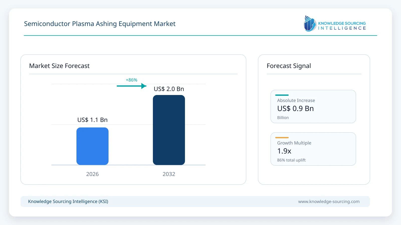
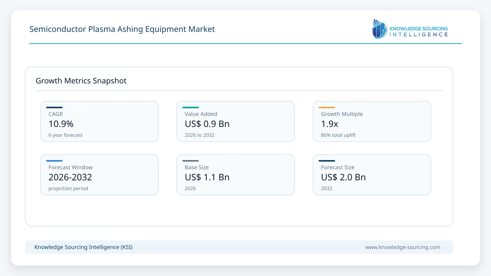
The Semiconductor Plasma Ashing Equipment Market is estimated at USD 1.10 billion in 2026 and is projected to reach USD 2.05 billion by 2032, representing a CAGR of 10.9% during 2026-2032.
Highlights:
- 1Dry strip remains a core front-end process after lithography, implantation and plasma etching.
- 2Remote and downstream plasma architectures gain importance where device damage and charging must be minimized.
- 3High-dose implant strip and difficult polymer removal increase process complexity and equipment value.
- 4Advanced packaging creates new demand for descum, polyimide strip and large-area panel plasma processing.
- 5Asia Pacific remains the largest opportunity because it combines leading fabs, memory production and packaging capacity.
Market Overview
Plasma ashing typically uses oxygen-containing chemistries to convert organic photoresist into volatile reaction products that can be evacuated from the process chamber. More demanding applications add hydrogen, fluorine-bearing or mixed chemistries to remove implant-hardened resist, post-etch polymers or specialty organic films. Remote and downstream sources separate the wafer from the highest-energy plasma region, reducing ion bombardment and electrical damage while maintaining radical density for chemical removal.
Front-end systems are optimized for high wafer throughput, uniform strip rate and compatibility with 200 mm or 300 mm manufacturing. High-dose implant strip is particularly challenging because ion implantation can carbonize and densify the resist surface, making conventional oxygen ash less effective. Low-k dielectrics, sensitive gate stacks and advanced interconnect materials also place tighter limits on plasma-induced damage and material loss. These requirements support microwave, inductively coupled and downstream plasma configurations with tighter temperature and chemistry control.
Advanced packaging adds a different set of requirements. Redistribution-layer lithography, bumping, fan-out wafer-level packaging and panel-level packaging require descum, polyimide strip, residue removal and surface preparation across thin wafers, carriers and increasingly large rectangular panels. As panel sizes increase, chamber uniformity, substrate handling and low-temperature processing become critical. The result is a market spanning mature high-volume front-end strip equipment and faster-growing packaging-oriented plasma systems.
Market Drivers
Advanced nodes require lower-damage dry strip
Leading-edge logic and memory contain increasingly sensitive low-k dielectrics, metal stacks and three-dimensional structures. Resist and polymer removal must therefore achieve high selectivity without plasma charging, excessive ion bombardment or material loss. Remote, downstream and microwave plasma sources are favored for these applications because they can provide high radical density while reducing direct ion exposure. ULVAC's NA-1300, for example, is positioned for damage-free high-dose ion-implant stripping and polymer removal on 200 mm and 300 mm wafers.
High-dose implant and post-etch residues increase process intensity
Ion implantation and aggressive plasma etching can harden photoresist and create fluorocarbon or organometallic residues that are difficult to remove. These films can require multi-step chemistries, higher temperatures or specialized plasma conditions. As device structures become more complex, fabs require ashers that can switch between normal photoresist strip, high-dose implant strip, residue removal and selective organic-film removal without increasing defectivity or chamber maintenance.
Advanced packaging expands descum and large-area plasma demand
Fan-out wafer-level packaging, redistribution layers, through-mold vias and panel-level packaging use thick resists, polyimides and polymer dielectrics that require controlled descum and strip. ASE announced a 310 mm x 310 mm automated panel-level packaging line in 2026, illustrating the industry's move toward larger substrate formats. ULVAC's NA-1500 and Nordson's ExoSPHERE target this shift with large-area plasma processing, while other suppliers are introducing panel-scale descum systems.
Productivity and cleanroom-floor efficiency remain strong purchase criteria
Ashing is repeated many times in semiconductor fabrication, so throughput, uptime and footprint have a direct effect on fab economics. Equipment vendors therefore emphasize multi-chamber layouts, fast wafer handling, compact footprints and high strip rates. ULVAC's ENVIRO-Optima is designed to replace several legacy systems within a smaller floor area, while PSK positions its SUPRA family around high throughput and low cost of ownership. Replacement demand is supported when new platforms can raise wafers per hour without requiring additional cleanroom space.
Restraints and Adoption Challenges
The principal challenge is balancing strip rate with material protection. More aggressive plasma conditions can increase throughput but also raise the risk of charging, low-k damage, metal oxidation or substrate heating. Difficult implant-hardened resist and post-etch polymers may require chemistries that increase chamber corrosion or maintenance. Packaging applications add substrate warpage, carrier compatibility and large-area uniformity requirements. Mature fabs also operate substantial installed bases of legacy ashers, so new equipment must demonstrate a clear productivity, defectivity or operating-cost advantage before replacement.
Segment Analysis
By Process Architecture
Remote and downstream plasma ashers represent the core high-volume category because they support low-damage resist removal across advanced logic, memory and specialty semiconductor production. Microwave sources are important for low-damage stripping and high-dose implant applications, while inductively coupled plasma configurations offer high radical density and process flexibility. Direct plasma systems remain relevant in packaging, R&D and less damage-sensitive processes where surface activation, descum and strip are combined in one chamber.
The fastest product evolution is occurring in advanced-packaging systems. Wafer-level platforms must handle 300 mm wafers, bonded carriers and thick polymer films, while panel-level systems require uniform treatment across substantially larger rectangular substrates. Low-temperature processing and non-contact handling become important where thin substrates or temporary-bond materials are used.
Architecture | Primary Strength | Typical Applications | Commercial Direction |
Remote/downstream plasma | Low ion damage with high radical density | FEOL strip, implant strip, polymer removal | Core advanced-wafer architecture |
Microwave plasma | Low-damage high-density radicals | High-dose implant strip, critical PR removal | Important in sensitive advanced devices |
ICP-based downstream | High throughput and chemistry flexibility | High-volume resist strip, residue removal | Expanding in compact high-productivity platforms |
Direct RF plasma | Flexible ion/radical interaction | Descum, packaging clean, surface treatment | Common in packaging and specialty fabs |
Multi-chamber wafer systems | High WPH and uptime | 300 mm volume manufacturing | Favored for fab productivity |
Large-area panel systems | Uniform processing on rectangular substrates | FO-PLP descum, strip and surface prep | Fast-growing advanced-packaging category |
Market and Technology Indicators
Indicator | Current Evidence | Market Impact |
Foundry dry-asher order | Acmewin announced AIBO II FEOL verification and a Taiwan foundry order in February 2026. | Shows additional suppliers gaining qualification in front-end dry strip. |
Repeat MEMS shipment | Acmewin shipped another AIBO II system to a Taiwan MEMS manufacturer in May 2026. | Supports replacement and specialty-fab demand for 6-inch and 8-inch ashers. |
Panel-level plasma launch | Nordson highlighted the new MARCH ExoSPHERE at SEMICON Taiwan 2026. | Extends plasma treatment toward larger panel and wafer formats. |
310 mm panel production line | ASE announced a 310 mm x 310 mm automated PLP line in May 2026, with production planned in 2027. | Creates new demand for large-area descum, strip and surface-treatment tools. |
FO-PLP ashing platform | ULVAC's NA-1500 handles roughly 500 mm-class square substrates at low process temperature. | Confirms dedicated equipment architecture for panel-level packaging. |
Dry-strip specialization | PSK's current portfolio centers on SUPRA dry strip, NHM strip, dry clean and edge clean. | Keeps specialist dry-strip vendors central to front-end competition. |
Regional Opportunity
Asia Pacific
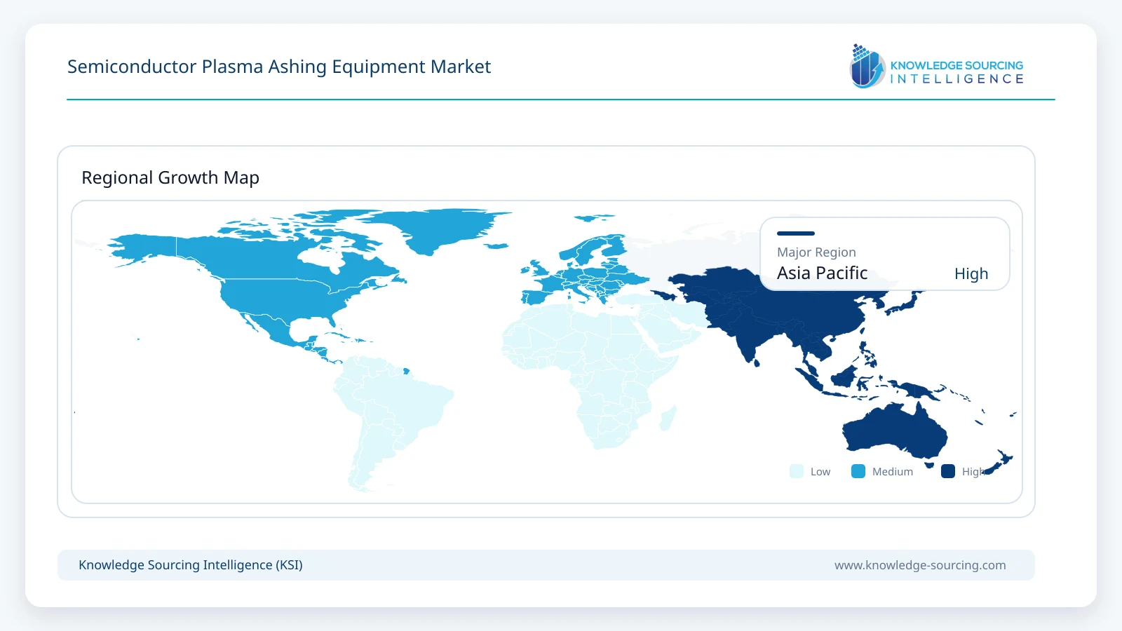
Asia Pacific is the largest market for semiconductor plasma ashing equipment because Taiwan, South Korea, China, Japan and Southeast Asia contain the majority of global wafer fabrication and advanced packaging capacity. Plasma strip is required repeatedly across logic, DRAM, NAND, foundry, MEMS and power-semiconductor production, creating a large installed base and regular replacement cycle. The region also contains several major equipment suppliers, including PSK, ULVAC, Acmewin and a growing group of packaging-plasma specialists.
South Korea is important both as a demand center and supply base. Samsung Electronics and SK hynix operate large advanced logic and memory fabs, while PSK has built its position around dry strip, dry cleaning, hard-mask strip and wafer-edge processing. Taiwan combines TSMC's leading-edge foundry capacity with one of the world's deepest OSAT and packaging ecosystems. Acmewin's 2026 AIBO II orders demonstrate active local qualification of dry-strip equipment, while ASE's panel-level packaging expansion creates a new demand layer for large-area plasma descum and cleaning.
Japan remains important through ULVAC and other plasma-equipment and component suppliers, and through a diversified semiconductor base spanning logic, image sensors, power devices and specialty wafers. China continues to add domestic wafer-fab and packaging capacity and is a major target market for global plasma-system suppliers. Southeast Asia contributes through assembly, test and packaging investment, where plasma cleaning and descum are used before bonding, molding, underfill and metallization.
North America remains relevant through logic, memory, analog and specialty fabs as well as R&D and advanced packaging. Europe contributes through automotive, power-semiconductor, MEMS and specialty-device manufacturing. Both regions also generate replacement demand for mature 150 mm and 200 mm lines.
Competitive Landscape
The competitive landscape combines front-end dry-strip specialists with broader plasma-processing and packaging-equipment suppliers. PSK is highly focused on dry strip and related semiconductor surface-processing steps, while ULVAC offers a broad portfolio covering 100 mm to 300 mm wafer ashers and panel-level packaging systems. Acmewin is expanding its AIBO platform in Taiwan, particularly for 6-inch and 8-inch fabs.
Nordson MARCH competes strongly in wafer-level and panel-level packaging plasma treatment, with systems for descum, stripping, cleaning and surface activation. Yield Engineering Systems (YES) offers precision strip and descum platforms for wafers up to 200 mm, while PVA TePla provides plasma ashing and cleaning equipment across R&D and production. Other participants include Plasma-Therm, Samco, Advanced Energy-supported OEM ecosystems, SPTS Technologies / KLA in adjacent plasma processing, and regional system suppliers serving MEMS, power devices and packaging.
Major companies and ecosystem participants covered: PSK, ULVAC, Nordson MARCH, Acmewin International, Yield Engineering Systems, PVA TePla, Plasma-Therm, Samco, AREESYS, Astro Plasma, SPTS Technologies / KLA, Tokyo Electron ecosystem suppliers, Hitachi High-Tech ecosystem suppliers, Advanced Energy and regional refurbished-equipment specialists.
Recent Developments
August 2026: Nordson highlighted its new MARCH ExoSPHERE plasma treatment system for panels and wafers at SEMICON Taiwan 2026.
May 2026: Acmewin shipped another AIBO II dry asher to a leading Taiwan MEMS manufacturer after customer evaluation.
May 2026: ASE announced an automated 310 mm x 310 mm panel-level packaging line, with production expected in the first half of 2027.
February 2026: Acmewin announced FEOL verification of the AIBO II dry asher and its first customer order of the year from a Taiwan wafer foundry.
2026: ULVAC continued commercialization of the NA-1500 for fan-out panel-level packaging, supporting roughly 500 mm-class square substrates.
2026: SEMICON Taiwan exhibitors presented new large-area descum platforms using remote plasma and RF bias for panel-level packaging.
Semiconductor Plasma Ashing Equipment Market Scope
| Report Metric | Details |
|---|---|
| Total Market Size in 2026 | USD 1.10 billion |
| Total Market Size in 2032 | USD 2.05 billion |
| Forecast Unit | Billion |
| Growth Rate | 10.9% |
| Study Period | 2021 to 2032 |
| Historical Data | 2021 to 2024 |
| Base Year | 2025 |
| Forecast Period | 2026 – 2032 |
| Segmentation | Process Architecture, Application, Manufacturing Stage, Substrate Format, End Device, Geography |
| Companies |
|
Market Segmentation
By Process Architecture
Remote/Downstream Plasma Ashers
Microwave Plasma Ashers
ICP-Based Strip Systems
Direct RF Plasma Systems
Multi-Chamber Wafer Platforms
Large-Area Panel Systems
By Application
Standard Photoresist Strip
High-Dose Implant Resist Strip
Post-Etch Polymer Removal
Descum
Polyimide and Thick-Resist Strip
Surface Preparation and Organic Residue Removal
By Manufacturing Stage
Front-End Wafer Fabrication
MEMS and Specialty Devices
Wafer-Level Packaging
Fan-Out Wafer-Level Packaging
Panel-Level Packaging
By Substrate Format
300 mm Wafers
200 mm Wafers
150 mm and Smaller Wafers
Wafer Carriers and Frames
Large-Area Panels
By End Device
Logic and Foundry
DRAM
NAND
Power Semiconductors
MEMS and Sensors
Advanced Packaging
By Geography
Asia Pacific
Taiwan
South Korea
Japan
China
Southeast Asia
North America
Europe
Rest of World
Table of Contents
1. EXECUTIVE SUMMARY
1.1. Market Opportunity and Key Findings
1.2. Dry Strip and Ashing Outlook
1.3. Advanced Packaging Plasma Processing
2. MARKET OVERVIEW
2.1. Plasma Ashing Process Fundamentals
2.2. Resist Strip versus Descum
2.3. Remote and Downstream Plasma Sources
2.4. High-Dose Implant Strip
2.5. Post-Etch Polymer and Residue Removal
3. MARKET SIZE AND FORECAST, 2026-2032
3.1. Global Market Revenue
3.2. Annual Growth Analysis
3.3. Equipment, Service and Lifecycle Revenue
4. MARKET BY PROCESS ARCHITECTURE
4.1. Remote/Downstream Plasma Ashers
4.2. Microwave Plasma Ashers
4.3. ICP-Based Strip Systems
4.4. Direct RF Plasma Systems
4.5. Multi-Chamber Wafer Platforms
4.6. Large-Area Panel Systems
5. MARKET BY APPLICATION
5.1. Standard Photoresist Strip
5.2. High-Dose Implant Resist Strip
5.3. Post-Etch Polymer Removal
5.4. Descum
5.5. Polyimide and Thick-Resist Strip
5.6. Surface Preparation and Organic Residue Removal
6. MARKET BY MANUFACTURING STAGE
6.1. Front-End Wafer Fabrication
6.2. MEMS and Specialty Devices
6.3. Wafer-Level Packaging
6.4. Fan-Out Wafer-Level Packaging
6.5. Panel-Level Packaging
7. MARKET BY SUBSTRATE FORMAT
7.1. 300 mm Wafers
7.2. 200 mm Wafers
7.3. 150 mm and Smaller Wafers
7.4. Wafer Carriers and Frames
7.5. Large-Area Panels
8. MARKET BY END DEVICE
8.1. Logic and Foundry
8.2. DRAM
8.3. NAND
8.4. Power Semiconductors
8.5. MEMS and Sensors
8.6. Advanced Packaging
9. REGIONAL MARKET
9.1. Asia Pacific
9.1.1. Taiwan
9.1.2. South Korea
9.1.3. Japan
9.1.4. China
9.1.5. Southeast Asia
9.2. North America
9.3. Europe
9.4. Rest of World
10. MARKET DYNAMICS
10.1. Drivers
10.1.1. Low-Damage Advanced-Node Strip
10.1.2. High-Dose Implant and Polymer Residues
10.1.3. Advanced Packaging Expansion
10.1.4. Throughput and Footprint Optimization
10.2. Restraints
10.2.1. Plasma-Induced Damage Risk
10.2.2. Chemistry and Chamber-Maintenance Complexity
10.2.3. Large Installed Base of Legacy Ashers
10.2.4. Substrate Handling and Panel Uniformity
11. COMPETITIVE LANDSCAPE
11.1. Front-End Dry-Strip Specialists
11.2. Advanced-Packaging Plasma Suppliers
11.3. Large-Area Panel Strategies
11.4. Service, Refurbishment and Installed Base
12. COMPANY PROFILES
12.1. PSK
12.2. ULVAC
12.3. Nordson MARCH
12.4. Acmewin International
12.5. Yield Engineering Systems
12.6. PVA TePla
12.7. Plasma-Therm
12.8. Samco
12.9. AREESYS
12.10. Astro Plasma
12.11. KLA Corporation
12.12. Tokyo Electron ecosystem suppliers
12.13. Hitachi High-Tech ecosystem suppliers
12.14. Advanced Energy
13. RECENT DEVELOPMENTS
14. APPENDIX
Navigate
Trusted by the world's leading organizations











