
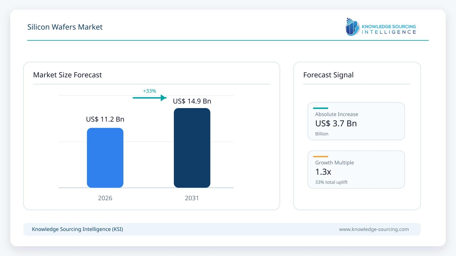
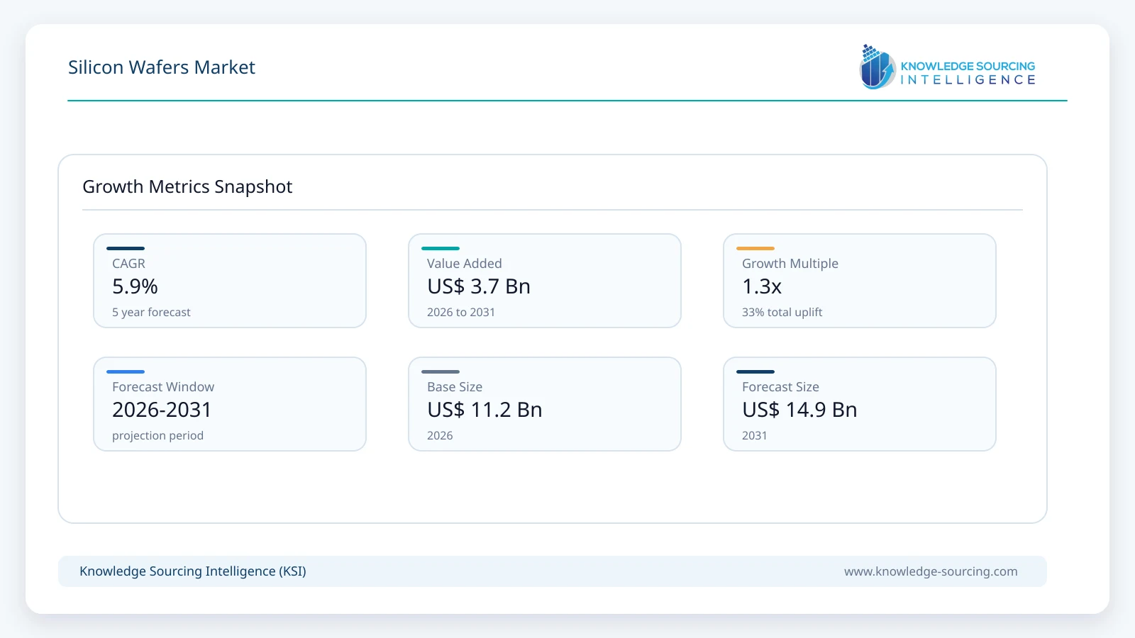
The Silicon Wafers Market is forecast to grow at a CAGR of 5.9%, reaching USD 14.9 billion in 2031 from USD 11.2 billion in 2026.
Highlights:
- 1AI infrastructure investment is reshaping demand toward high-specification 300 mm silicon wafers.
- 2Semiconductor supply chains continue balancing advanced-node expansion with mature-node inventory normalization.
- 3Wafer manufacturers are prioritizing quality, yield, and long-term customer qualification over rapid capacity additions.
- 4Automotive electrification, industrial automation, and high-performance computing broaden application demand beyond consumer electronics.
- 5Regional semiconductor policies continue influencing production localization and wafer procurement strategies.
Market Overview
Demand is determined less by consumer device shipments alone and more by fab utilization, technology-node migration, memory investment cycles, automotive semiconductor content, and the pace of capacity expansion at foundries and integrated device manufacturers. Consequently, purchasing decisions increasingly reflect long-term manufacturing roadmaps rather than short-term electronics demand.
The market entered the forecast period following a gradual recovery from the inventory correction experienced across several mature semiconductor segments. According to SEMI, worldwide silicon wafer shipments increased during 2025, supported primarily by demand for advanced logic and high-bandwidth memory serving artificial intelligence workloads, while traditional semiconductor applications recovered more gradually. The divergence between advanced and mature technology nodes continues to shape purchasing behavior and pricing across wafer categories.
Buyers increasingly prioritize wafer flatness, defect density, crystal quality, resistivity control, and supply reliability over price alone. Long qualification cycles and process compatibility make supplier switching costly, particularly for advanced-node manufacturing where wafer consistency directly affects yield. As a result, long-term commercial relationships remain an important feature of the industry.
Commercial value is distributed unevenly across wafer types. Standard wafers continue serving mature semiconductor production, while premium pricing is concentrated in larger-diameter polished, epitaxial, and specialty wafers supporting advanced logic, memory, automotive power devices, and emerging AI infrastructure. During the 2026–2031 forecast period, investment decisions are expected to remain closely linked to semiconductor fabrication capacity, technology migration, government-backed manufacturing programs, and sustained demand for data center computing.
Key Market Indicators
Indicator | Latest Evidence | Commercial Meaning |
Worldwide silicon wafer shipments | 12,973 million square inches (2025) | Shipment recovery indicates improving semiconductor production activity. |
Worldwide wafer revenue | US$11.4 billion (2025) | Pricing pressure remains despite improving shipment volumes. |
Annual shipment growth | 5.8% (2025) | Recovery is concentrated in advanced semiconductor applications. |
Q1 2026 shipment growth | 13.1% year-on-year | AI-driven semiconductor production continues strengthening wafer demand. |
Primary demand catalyst | AI logic and HBM production | Advanced-node capacity expansion supports premium wafer consumption. |
Key indicator: Worldwide silicon wafer shipments reached 12,973 million square inches in 2025.
Commercial meaning: Demand recovery is increasingly concentrated in advanced semiconductor manufacturing rather than across all end-use markets.
Market Drivers
Expansion of AI data centers is increasing demand for advanced 300 mm wafers
Artificial intelligence infrastructure has become one of the strongest demand sources for advanced silicon wafers. Investments in AI accelerators, high-bandwidth memory, advanced logic processors, and hyperscale data centers require larger-diameter wafers capable of supporting sub-3 nm manufacturing processes. SEMI reported that demand for polished 300 mm wafers and advanced epitaxial wafers strengthened throughout 2025 because of AI-related semiconductor production, while shipment growth continued into early 2026. Wafer suppliers are responding by prioritizing advanced manufacturing capability, customer qualification, and process consistency rather than pursuing broad-based capacity expansion.
Government-backed semiconductor manufacturing programs are expanding wafer consumption
National semiconductor policies continue encouraging new fabrication capacity across Asia Pacific, North America, and Europe. Public funding programs supporting domestic semiconductor manufacturing increase demand for silicon wafers during fab construction, process qualification, and volume production. New facilities require long-term wafer supply agreements before commercial production begins, creating predictable procurement cycles for wafer manufacturers. The resulting demand extends beyond logic foundries to memory, power semiconductor, and specialty device production, allowing suppliers to diversify their customer base while reducing dependence on individual application segments.
Automotive semiconductor content continues increasing wafer requirements
Vehicle electrification, advanced driver assistance systems, power management, battery control, and onboard connectivity have raised semiconductor content per vehicle. These applications depend on reliable silicon substrates capable of meeting stringent quality and lifetime requirements. Automotive customers also impose extensive qualification standards, making wafer quality and process consistency central purchasing criteria. Although automotive semiconductor demand experienced inventory adjustments during the recent industry slowdown, SEMI notes that mature-node inventories have begun normalizing, supporting a gradual recovery in wafer procurement for automotive and industrial applications.
Long-term investment by wafer manufacturers supports future semiconductor capacity
Wafer manufacturers continue investing selectively despite cyclical market conditions. Rather than expanding capacity indiscriminately, suppliers increasingly focus on technology upgrades, process optimization, and advanced 300 mm production. Siltronic's latest annual report notes stronger demand for 300 mm products driven by AI servers and increased customer qualification activity at its Singapore fabrication facility, while also acknowledging ongoing pricing pressure outside long-term agreements. Such investments strengthen supply capability for advanced semiconductor manufacturing while improving production efficiency and yield over the longer term.
Market Restraints and Challenges
Lengthy qualification cycles restrict supplier switching and delay revenue realization
Silicon wafers become part of tightly controlled semiconductor manufacturing processes, requiring extensive qualification before commercial production. Any change in wafer supplier can trigger process validation, reliability testing, and yield optimization that may take several months. This affects both integrated device manufacturers and foundries, particularly for advanced logic and automotive semiconductors where process stability is critical. Several wafer producers, including Siltronic and SUMCO, continue to identify customer qualification timelines as an important factor influencing capacity utilization and revenue realization, making demand recovery slower than improvements in semiconductor orders alone. Official company disclosures also indicate that customer approvals remain closely linked to technology node transitions and new fab ramp-ups.
Persistent pricing pressure in mature-node applications limits margin improvement
Although wafer shipments have recovered from the semiconductor inventory correction, pricing conditions remain uneven across wafer categories. SEMI reported higher shipment volumes during 2025 while industry revenue remained below earlier cyclical peaks, indicating continued price pressure across portions of the market. Mature-node devices used in consumer electronics, industrial equipment, and conventional computing continue facing cautious purchasing as customers normalize inventories. Several manufacturers have highlighted that long-term agreements provide greater pricing stability than spot transactions, but competition remains intense for standard wafer products where technical differentiation is comparatively limited. These conditions primarily affect suppliers serving mature semiconductor applications rather than companies focused on advanced-node production.
Capital-intensive manufacturing raises barriers to expansion
Silicon wafer manufacturing requires highly automated crystal growth, slicing, polishing, inspection, and contamination-control processes that demand continuous capital investment. Expansion projects also require long construction periods, specialized equipment, and experienced technical personnel before commercial output can begin. Company annual reports from Siltronic, SUMCO, and Shin-Etsu Chemical indicate that investment decisions are increasingly linked to confirmed customer commitments rather than speculative demand. As a result, suppliers generally expand capacity in phases, reducing the risk of oversupply but extending the time required to respond to sudden increases in semiconductor production. Smaller manufacturers often face greater financing constraints when competing with established global suppliers.
Geopolitical trade restrictions complicate supply-chain planning
The semiconductor industry continues adjusting to export controls, regional industrial policies, and localization initiatives affecting technology supply chains. While silicon wafers themselves are less exposed than advanced semiconductor equipment, customers increasingly seek geographically diversified supply to reduce operational risk. Wafer manufacturers therefore face pressure to maintain production capability across multiple regions while complying with evolving trade regulations. These adjustments increase logistics complexity, inventory planning requirements, and operating costs, particularly for suppliers supporting multinational semiconductor fabrication networks.
Major Segment Analysis
300 mm Wafers
The 300 mm wafer segment represents the most commercially important category within the silicon wafer market because it supports advanced logic processors, high-performance memory, AI accelerators, and many leading-edge semiconductor manufacturing processes. Larger wafer diameters allow substantially higher chip output per production cycle than smaller formats, improving manufacturing efficiency and reducing cost per die for high-volume fabrication. As semiconductor companies continue investing in artificial intelligence infrastructure, demand for premium-quality 300 mm wafers remains closely aligned with advanced foundry and memory expansion.
Purchasing decisions within this segment extend beyond wafer pricing. Foundries and integrated device manufacturers evaluate crystal uniformity, defect density, surface flatness, oxygen concentration, and long-term supply assurance before approving suppliers. Qualification periods remain lengthy because even minor variations can affect manufacturing yield and device performance. Consequently, competition increasingly centers on production consistency, process capability, and customer relationships rather than price alone.
Although 200 mm wafers continue serving automotive, industrial, and power semiconductor applications, investment activity across the forecast period is expected to remain concentrated around advanced 300 mm manufacturing. Suppliers capable of maintaining high production yields while supporting advanced technology nodes are likely to capture a larger share of value creation within the broader silicon wafer industry.
Regional Analysis
Region | Main Demand Signal | Principal Constraint |
North America | AI semiconductor investment, advanced foundries, CHIPS Act projects | High construction and labor costs |
Europe | Automotive semiconductors, industrial electronics, regional semiconductor programs | Energy costs and slower fab expansion |
Asia Pacific | Global semiconductor manufacturing concentration, memory and foundry capacity | Geopolitical trade uncertainty and cyclical demand |
Middle East and Africa | Emerging semiconductor design ecosystem and electronics investment | Limited domestic wafer manufacturing capacity |
North America
The United States continues strengthening domestic semiconductor manufacturing through investments supported by the CHIPS and Science Act. New fabrication projects announced by Intel, TSMC, Samsung Electronics, GlobalFoundries, and Micron increase long-term demand for high-quality silicon wafers during facility qualification and commercial production. AI infrastructure investment further supports procurement of advanced 300 mm wafers used in logic processors and high-bandwidth memory. Canada and Mexico contribute primarily through semiconductor packaging, electronics manufacturing, automotive production, and cross-border supply-chain integration rather than large-scale wafer fabrication.
Europe
European demand remains closely linked to automotive electronics, industrial automation, medical devices, and power semiconductor manufacturing. Germany continues serving as the region's principal semiconductor manufacturing hub, while France, Italy, and the United Kingdom maintain important positions in automotive, industrial, and research-intensive semiconductor activities. The European Chips Act continues supporting regional manufacturing resilience by encouraging investment across semiconductor value chains. Nevertheless, relatively high energy costs and extended project development timelines may moderate the pace of new wafer production compared with Asia Pacific.
Asia Pacific
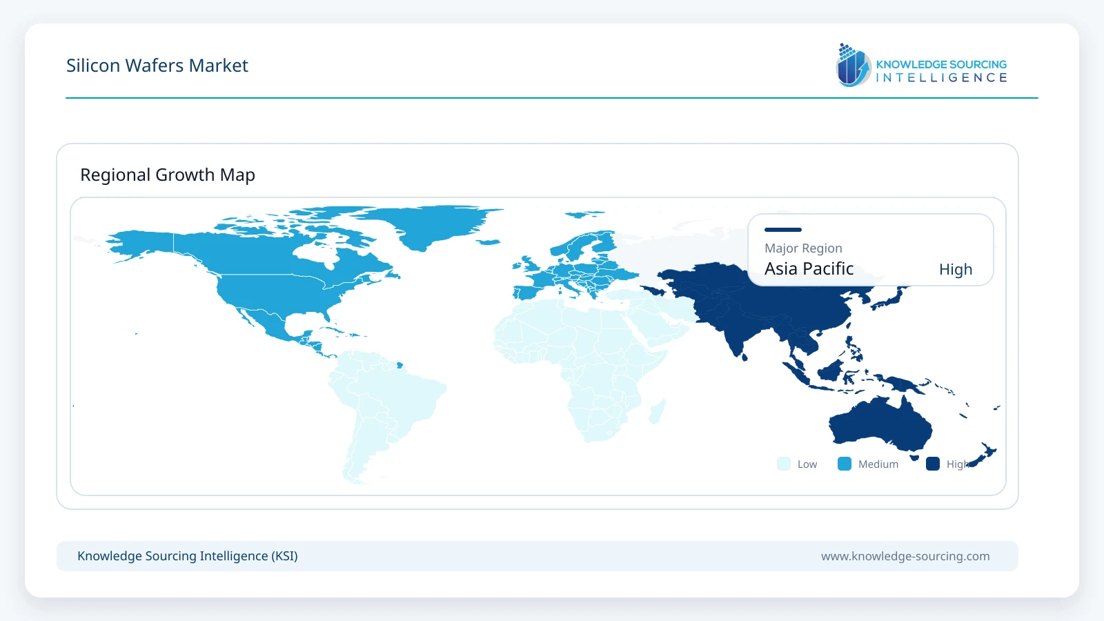
Asia Pacific remains the operational center of the global silicon wafer ecosystem because it combines large-scale wafer production with the world's highest concentration of semiconductor fabrication facilities. Taiwan, South Korea, Japan, China, and Singapore collectively account for much of global foundry, memory, and wafer manufacturing capacity. Japan hosts several leading silicon wafer manufacturers, including Shin-Etsu Chemical, SUMCO, and Tokuyama, while Taiwan and South Korea remain central to advanced logic and memory production. China continues expanding domestic semiconductor manufacturing through government-backed investment, and India is strengthening its semiconductor ecosystem through fabrication incentives and assembly initiatives. Continued investment in AI computing, cloud infrastructure, and advanced packaging supports regional wafer demand despite periodic inventory corrections.
Middle East and Africa
Commercial activity across the Middle East and Africa remains concentrated in semiconductor design, electronics manufacturing, research, and technology investment rather than silicon wafer production. Israel maintains an important semiconductor development ecosystem supported by multinational technology companies and advanced research institutions. Saudi Arabia and the United Arab Emirates continue investing in digital infrastructure, artificial intelligence, and electronics manufacturing capabilities that may gradually increase semiconductor consumption. However, the region remains heavily dependent on imported silicon wafers because domestic manufacturing capacity is limited, making supply security and international trade relationships important purchasing considerations.
Competitive Landscape
The silicon wafers market remains relatively consolidated, with a limited number of manufacturers supplying the ultra-high-quality wafers required for advanced semiconductor fabrication. High capital requirements, stringent customer qualification procedures, intellectual property, manufacturing yield, and decades of process expertise create substantial barriers to entry. Long-term supply agreements further strengthen relationships between wafer suppliers and semiconductor manufacturers, making supplier replacement uncommon once production qualification has been completed.
Shin-Etsu Chemical Co., Ltd., SUMCO Corporation, Siltronic AG, GlobalWafers Co., Ltd., SK Siltron, Soitec, Okmetic, Wafer Works Corporation, and Tokuyama Corporation compete through manufacturing capability, crystal growth technology, wafer quality, geographic production footprint, and long-term customer partnerships rather than price alone. Product differentiation is particularly important for advanced 300 mm wafers, epitaxial wafers, and specialty substrates supporting AI processors, automotive semiconductors, power electronics, and high-performance memory.
Recent investment strategies show a common industry response to changing semiconductor demand. Rather than pursuing aggressive capacity expansion across all wafer categories, suppliers are prioritizing advanced manufacturing technologies, productivity improvements, automation, and selective investments aligned with confirmed customer demand. Several companies are also expanding regional production footprints and strengthening supply-chain resilience to reduce operational risk associated with geopolitical uncertainty and evolving semiconductor industrial policies.
Recent Developments
March 2026 – Soitec extends NSIG wafer licensing partnership: Soitec signed a 10-year extension of its manufacturing and commercial licensing framework with National Silicon Industry Group (NSIG), reinforcing silicon-on-insulator (SOI) wafer production and intellectual property protection for the Chinese semiconductor market.
March 2026 – Soitec secures multi-year POI wafer supply agreement with Skyworks: Soitec signed a long-term agreement to supply Piezoelectric-on-Insulator (POI) wafers for Skyworks’ Sky5 platform, supporting high-volume RF filter production for advanced 5G smartphones and next-generation wireless devices.
February 2026 – Okmetic begins volume production from expanded Vantaa wafer fab: Okmetic started volume production at its expanded Finland facility, significantly increasing 200 mm polished silicon wafer capacity for MEMS, RF, power semiconductor, and silicon-on-insulator wafer applications.
May 2025 – GlobalWafers opens first U.S. 300 mm silicon wafer facility: GlobalWafers inaugurated its Sherman, Texas, plant, the first U.S. facility producing advanced 300 mm silicon wafers in over two decades, strengthening domestic semiconductor material supply chains.
Regulatory and Policy Environment
Government industrial policy continues influencing investment decisions across the global silicon wafer value chain. Public funding programs supporting semiconductor manufacturing in the United States, Europe, Japan, South Korea, China, and India encourage new fabrication facilities that ultimately increase demand for silicon wafers during qualification, pilot production, and commercial ramp-up. Although these initiatives primarily target semiconductor manufacturing rather than wafer production itself, substrate suppliers benefit from the resulting expansion of fabrication capacity.
Policy frameworks increasingly emphasize supply-chain resilience alongside manufacturing growth. Export controls affecting semiconductor technologies, localization requirements, and national security considerations have encouraged semiconductor companies to diversify sourcing strategies and reduce dependence on individual manufacturing locations. Wafer suppliers are therefore expanding regional manufacturing capability and strengthening supply continuity while maintaining compliance with changing trade regulations.
Environmental requirements also continue shaping production practices. Silicon wafer manufacturing requires considerable energy, ultra-pure water, and precision chemical processing. Consequently, manufacturers are investing in energy efficiency, water recycling, emissions reduction, and responsible chemical management to satisfy regulatory obligations and customer sustainability requirements. These initiatives increasingly influence supplier qualification, particularly among global semiconductor manufacturers that have established environmental performance targets throughout their supply chains.
Outlook and Strategic Implications
Demand during the 2026–2031 forecast period is expected to remain closely associated with semiconductor fabrication investment rather than consumer electronics shipments alone. Artificial intelligence infrastructure, advanced memory, high-performance computing, automotive electrification, industrial automation, and next-generation communications will continue supporting procurement of premium silicon wafers, particularly within advanced 300 mm production. At the same time, mature-node applications are likely to experience a steadier recovery as inventory normalization progresses across industrial and consumer markets.
Commercial performance will increasingly depend on manufacturing quality rather than production volume alone. Customers are expected to prioritize suppliers capable of delivering consistent crystal quality, stable process performance, dependable long-term supply, and close technical collaboration throughout product qualification. These factors strengthen the competitive position of established manufacturers with proven production capability and long-standing customer relationships.
Strategic priorities across the industry are expected to include:
Expansion of advanced 300 mm manufacturing capability aligned with confirmed customer demand.
Greater investment in process automation, yield improvement, and manufacturing efficiency to protect operating margins.
Diversification of production footprints to improve supply-chain resilience and address geopolitical risk.
Continued development of specialty wafers supporting automotive power devices, AI accelerators, advanced memory, and high-performance computing.
Closer collaboration between wafer suppliers, semiconductor manufacturers, equipment providers, and government-supported fabrication projects to shorten qualification timelines and improve long-term supply security.
While cyclical fluctuations in semiconductor demand will continue influencing shipment volumes, the industry's structural outlook remains supported by sustained investment in advanced computing infrastructure, semiconductor manufacturing capacity, and technology-intensive applications. Suppliers capable of maintaining high manufacturing yields, disciplined capital allocation, and reliable long-term customer support are expected to remain well positioned as semiconductor production continues shifting toward more complex and higher-value devices.
Silicon Wafers Market Scope:
| Report Metric | Details |
|---|---|
| Total Market Size in 2026 | USD 11.2 billion |
| Total Market Size in 2031 | USD 14.9 billion |
| Forecast Unit | USD Billion |
| Growth Rate | 5.9% |
| Study Period | 2021 to 2031 |
| Historical Data | 2021 to 2024 |
| Base Year | 2025 |
| Forecast Period | 2026 – 2031 |
| Segmentation | Wafer Size, Fabrication Method, Industry Vertical, Geography |
| Companies |
|
Market Segmentation
By Wafer Size
?100 mm
125 mm–150 mm
200 mm
300 mm
450 mm
By Fabrication Method
Czochralski (CZ)
Magnetic Czochralski (MCZ)
Float Zone (FZ)
Epitaxial Wafers
By Industry Vertical
Consumer Electronics
Automotive
Industrial
Telecommunications
Healthcare
Data Centers and AI
Others
By Geography
North America
USA
Canada
Mexico
South America
Brazil
Argentina
Others
Europe
France
Germany
UK
Italy
Others
Middle East and Africa
Saudi Arabia
UAE
Israel
Others
Asia Pacific
China
India
South Korea
Taiwan
Thailand
Indonesia
Japan
Others
Table of Contents
1. INTRODUCTION
1.1. Market Overview
1.2. Market Definition
1.3. Scope of the Study
1.4. Market Segmentation
1.5. Currency
1.6. Assumptions
1.7. Base and Forecast Years Timeline
1.8. Key Benefits to the Stakeholder
2. RESEARCH METHODOLOGY
2.1. Research Design
2.2. Research Processes
3. EXECUTIVE SUMMARY
3.1. Key Findings
3.2. CXO Perspective
4. MARKET DYNAMICS
4.1. Market Drivers
4.2. Market Restraints
4.3. Porter’s Five Forces Analysis
4.3.1. Bargaining Power of Suppliers
4.3.2. Bargaining Power of Buyers
4.3.3. Threat of New Entrants
4.3.4. Threat of Substitutes
4.3.5. Competitive Rivalry in the Industry
4.4. Industry Value Chain Analysis
4.5. Analyst View
5. SILICON WAFERS MARKET, BY WAFER SIZE
5.1. Introduction
5.2. ?100 mm
5.3. 125 mm–150 mm
5.4. 200 mm
5.5. 300 mm
5.6. 450 mm
6. SILICON WAFERS MARKET, BY FABRICATION METHOD
6.1. Introduction
6.2. Czochralski (CZ)
6.3. Magnetic Czochralski (MCZ)
6.4. Float Zone (FZ)
6.5. Epitaxial Wafers
7. SILICON WAFERS MARKET, BY INDUSTRY VERTICAL
7.1. Introduction
7.2. Consumer Electronics
7.3. Automotive
7.4. Industrial
7.5. Telecommunications
7.6. Healthcare
7.7. Data Centers and AI
7.8. Others
8. SILICON WAFERS MARKET, BY GEOGRAPHY
8.1. Introduction
8.2. North America
8.2.1. By Wafer Size
8.2.2. By Fabrication Method
8.2.3. By Industry Vertical
8.2.4. By Country
8.2.4.1. USA
8.2.4.1.1. Market Trends and Opportunities
8.2.4.1.2. Growth Prospects
8.2.4.2. Canada
8.2.4.2.1. Market Trends and Opportunities
8.2.4.2.2. Growth Prospects
8.2.4.3. Mexico
8.2.4.3.1. Market Trends and Opportunities
8.2.4.3.2. Growth Prospects
8.3. South America
8.3.1. By Wafer Size
8.3.2. By Fabrication Method
8.3.3. By Industry Vertical
8.3.4. By Country
8.3.4.1. Brazil
8.3.4.1.1. Market Trends and Opportunities
8.3.4.1.2. Growth Prospects
8.3.4.2. Argentina
8.3.4.2.1. Market Trends and Opportunities
8.3.4.2.2. Growth Prospects
8.3.4.3. Others
8.3.4.3.1. Market Trends and Opportunities
8.3.4.3.2. Growth Prospects
8.4. Europe
8.4.1. By Wafer Size
8.4.2. By Fabrication Method
8.4.3. By Industry Vertical
8.4.4. By Country
8.4.4.1. France
8.4.4.1.1. Market Trends and Opportunities
8.4.4.1.2. Growth Prospects
8.4.4.2. Germany
8.4.4.2.1. Market Trends and Opportunities
8.4.4.2.2. Growth Prospects
8.4.4.3. UK
8.4.4.3.1. Market Trends and Opportunities
8.4.4.3.2. Growth Prospects
8.4.4.4. Italy
8.4.4.4.1. Market Trends and Opportunities
8.4.4.4.2. Growth Prospects
8.4.4.5. Others
8.4.4.5.1. Market Trends and Opportunities
8.4.4.5.2. Growth Prospects
8.5. Middle East and Africa
8.5.1. By Wafer Size
8.5.2. By Fabrication Method
8.5.3. By Industry Vertical
8.5.4. By Country
8.5.4.1. Saudi Arabia
8.5.4.1.1. Market Trends and Opportunities
8.5.4.1.2. Growth Prospects
8.5.4.2. UAE
8.5.4.2.1. Market Trends and Opportunities
8.5.4.2.2. Growth Prospects
8.5.4.3. Israel
8.5.4.3.1. Market Trends and Opportunities
8.5.4.3.2. Growth Prospects
8.5.4.4. Others
8.5.4.4.1. Market Trends and Opportunities
8.5.4.4.2. Growth Prospects
8.6. Asia Pacific
8.6.1. By Wafer Size
8.6.2. By Fabrication Method
8.6.3. By Industry Vertical
8.6.4. By Country
8.6.4.1. China
8.6.4.1.1. Market Trends and Opportunities
8.6.4.1.2. Growth Prospects
8.6.4.2. India
8.6.4.2.1. Market Trends and Opportunities
8.6.4.2.2. Growth Prospects
8.6.4.3. South Korea
8.6.4.3.1. Market Trends and Opportunities
8.6.4.3.2. Growth Prospects
8.6.4.4. Taiwan
8.6.4.4.1. Market Trends and Opportunities
8.6.4.4.2. Growth Prospects
8.6.4.5. Thailand
8.6.4.5.1. Market Trends and Opportunities
8.6.4.5.2. Growth Prospects
8.6.4.6. Indonesia
8.6.4.6.1. Market Trends and Opportunities
8.6.4.6.2. Growth Prospects
8.6.4.7. Japan
8.6.4.7.1. Market Trends and Opportunities
8.6.4.7.2. Growth Prospects
8.6.4.8. Others
8.6.4.8.1. Market Trends and Opportunities
8.6.4.8.2. Growth Prospects
9. COMPETITIVE ENVIRONMENT AND ANALYSIS
9.1. Major Players and Strategy Analysis
9.2. Market Share Analysis
9.3. Mergers, Acquisitions, Agreements, and Collaborations
9.4. Competitive Dashboard
10. COMPANY PROFILES
10.1. Siltronic
10.2. Sumco Corporation
10.3. Shin-Etsu Chemical Co., Ltd.
10.4. Okmetic
10.5. GlobalWafers (Sino-American Silicon)
10.6. SK Siltron
10.7. Wafer Works Corporation
10.8. Soitec
10.9. Tokuyama Corporation
LIST OF FIGURES
LIST OF TABLES
Navigate
Trusted by the world's leading organizations











