Demand for Advanced Packaging Technologies to Fuel the Semiconductor Lead Frame Market

 Source: Semiconductor Industry Association
The growing use of alternative packaging technologies, such as fan-out wafer-level packaging (FOWLP) and system-in-package (SiP) solutions, is limiting semiconductor lead frame market growth. These technologies offer several advantages over traditional lead frame-based packaging, including higher levels of integration and improved thermal performance.
Some semiconductor and electronics businesses are migrating away from lead frame-based packaging solutions in favor of these alternatives, which are projected to slow the market over the projection period. Furthermore, the persistent scarcity of semiconductor components influences the semiconductor lead frame market since it affects the total demand for semiconductor devices and the components needed to create them, including lead frames. The scarcity raises prices and makes it more difficult for certain producers to obtain the materials and resources they need to create their products.
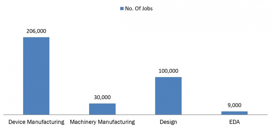
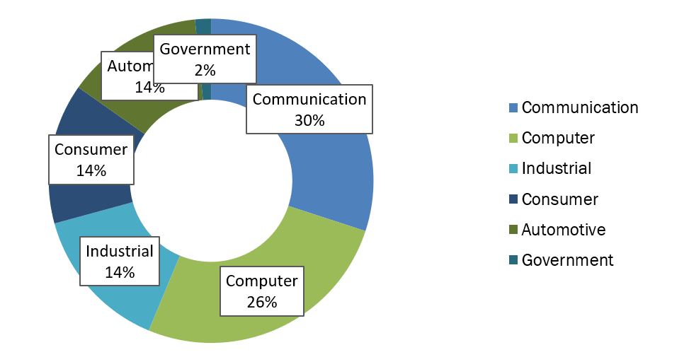
In 2022, semiconductor end-use sales in the industrial, consumer, and automotive industries saw fluctuations in market share. Historically, these industries accounted for one-third of total sales, but the recent rise in market share indicates shifts in demand that will drive the chip business for the next decade.
Innovation in the automotive, industrial, and consumer electronics industries ensures that the industry's growth continues, with revenues potentially reaching $1 trillion in 2030. To accommodate rising chip demand, semiconductor companies have spent billions of dollars in additional investments over the past decade.
Figure 2: Semiconductor Sales Based on End-Users, in Billion USD, 2022
Source: Semiconductor Industry Association
The growing use of alternative packaging technologies, such as fan-out wafer-level packaging (FOWLP) and system-in-package (SiP) solutions, is limiting semiconductor lead frame market growth. These technologies offer several advantages over traditional lead frame-based packaging, including higher levels of integration and improved thermal performance.
Some semiconductor and electronics businesses are migrating away from lead frame-based packaging solutions in favor of these alternatives, which are projected to slow the market over the projection period. Furthermore, the persistent scarcity of semiconductor components influences the semiconductor lead frame market since it affects the total demand for semiconductor devices and the components needed to create them, including lead frames. The scarcity raises prices and makes it more difficult for certain producers to obtain the materials and resources they need to create their products.
In 2022, semiconductor end-use sales in the industrial, consumer, and automotive industries saw fluctuations in market share. Historically, these industries accounted for one-third of total sales, but the recent rise in market share indicates shifts in demand that will drive the chip business for the next decade.
Innovation in the automotive, industrial, and consumer electronics industries ensures that the industry's growth continues, with revenues potentially reaching $1 trillion in 2030. To accommodate rising chip demand, semiconductor companies have spent billions of dollars in additional investments over the past decade.
Figure 2: Semiconductor Sales Based on End-Users, in Billion USD, 2022
 Source: Semiconductor Industry Association
The growing demand for electronic devices in industries such as automotive, consumer electronics, telecommunications, and healthcare is driving the demand for semiconductor lead frames. This is due to rapid technological advancements in semiconductor packaging techniques and materials that allow for smaller, lighter, and more efficient devices.
The semiconductor industry's expansion, fueled by advances in AI, IoT, 5G, and automotive electronics, is driving up demand for semiconductor lead frames. The rising usage of sophisticated packaging technologies such as system-in-package and fan-out wafer-level packaging helps to drive industry development.
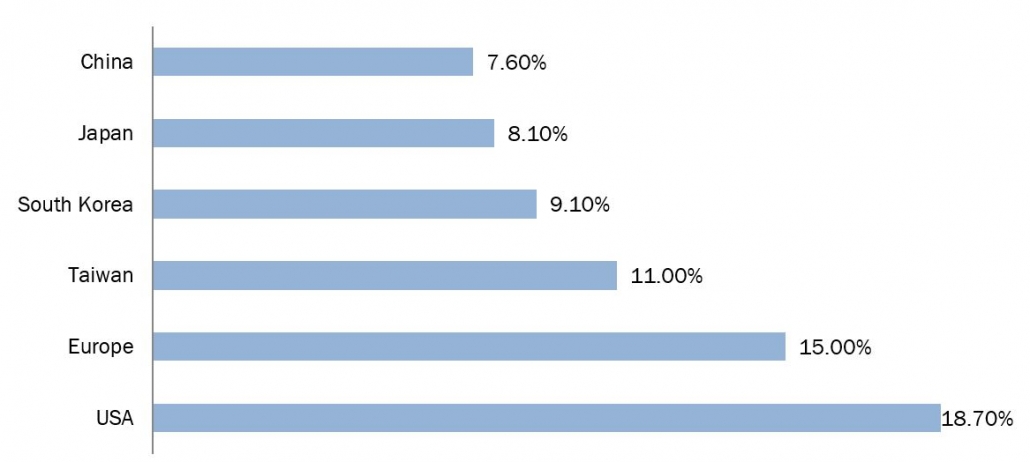
In terms of R&D investment as a percentage of revenue, the semiconductor business in the United States comes in second only behind pharmaceuticals and biotechnology. Despite increased worldwide rivalry, American companies invest more in R&D than any other country's semiconductor sector. This significant reinvestment fuels innovation, maintains worldwide sales industry leadership, and produces employment across the United States. According to SIA statistics, the United States spends 18.7%, whereas Europe spends 15.0%, Taiwan 11.0%, South Korea 9.1%, Japan 8.1%, and China 7.6%.
Figure 3: R&D Expenditures as a Percentage of Sales, 2022
Source: Semiconductor Industry Association
The growing demand for electronic devices in industries such as automotive, consumer electronics, telecommunications, and healthcare is driving the demand for semiconductor lead frames. This is due to rapid technological advancements in semiconductor packaging techniques and materials that allow for smaller, lighter, and more efficient devices.
The semiconductor industry's expansion, fueled by advances in AI, IoT, 5G, and automotive electronics, is driving up demand for semiconductor lead frames. The rising usage of sophisticated packaging technologies such as system-in-package and fan-out wafer-level packaging helps to drive industry development.
In terms of R&D investment as a percentage of revenue, the semiconductor business in the United States comes in second only behind pharmaceuticals and biotechnology. Despite increased worldwide rivalry, American companies invest more in R&D than any other country's semiconductor sector. This significant reinvestment fuels innovation, maintains worldwide sales industry leadership, and produces employment across the United States. According to SIA statistics, the United States spends 18.7%, whereas Europe spends 15.0%, Taiwan 11.0%, South Korea 9.1%, Japan 8.1%, and China 7.6%.
Figure 3: R&D Expenditures as a Percentage of Sales, 2022
 Source: Semiconductor Industry Association
The semiconductor industry expansion in various countries in the Asia Pacific region is expected to drive the semiconductor lead frame market. Rising demand for semiconductors is accompanied by an increase in demand for various equipment used to manufacture semiconductors, such as lead frames.
Semiconductor lead frames are essential in the packaging and connectivity of semiconductor devices. They provide dependable electrical connections and protect the sensitive semiconductor chip. The semiconductor application's unique needs and desired performance characteristics determine the lead frame design and material used.
In conclusion, Semiconductor lead frames are critical in the semiconductor packing process, allowing for the creation of high-performance electronic devices. Copper and its alloys are widely utilized because of their high electrical conductivity and thermal qualities, although iron-nickel alloys and composite materials may also be employed in specific applications.
Table 1: Key Developments
Source: Semiconductor Industry Association
The semiconductor industry expansion in various countries in the Asia Pacific region is expected to drive the semiconductor lead frame market. Rising demand for semiconductors is accompanied by an increase in demand for various equipment used to manufacture semiconductors, such as lead frames.
Semiconductor lead frames are essential in the packaging and connectivity of semiconductor devices. They provide dependable electrical connections and protect the sensitive semiconductor chip. The semiconductor application's unique needs and desired performance characteristics determine the lead frame design and material used.
In conclusion, Semiconductor lead frames are critical in the semiconductor packing process, allowing for the creation of high-performance electronic devices. Copper and its alloys are widely utilized because of their high electrical conductivity and thermal qualities, although iron-nickel alloys and composite materials may also be employed in specific applications.
Table 1: Key Developments
|
Year |
Development |
|
January 2024 |
TOPPAN Holdings agreed to buy 75% of KEYFIELDS' shares and form a subsidiary in February. As a result of the transfer, TOPPAN's digital transformation (DX) services in logistics will be strengthened, with a range of solutions available to address the rising need for logistics warehouse DX in Japanese and ASEAN markets. TOPPAN Group seeks to build its logistics DX business in Japan and the ASEAN area by developing end-to-end solutions and new business models. |
|
October 2023 |
Precision Micro increased manufacturing capacity at its Fort Dunlop plant in Birmingham, UK, by adding a second £1.8 million etch room. The room is equipped with three efficient etch machines and a semi-automated print frame, which are intended to reduce human intervention when printing photoresists onto bigger sheet metals up to 1500mm x 600mm. Customers benefit from this investment since it enhances throughput and lowers costs. |
Get in Touch
Interested in this topic? Contact our analysts for more details.
Latest Thought Articles

Top OSAT Companies Driving Semiconductor Assembly and Test Services Worldwide
Recently
EV Charging Stations Market Outlook: Smart Charging, Fast Charging, and Regional Expansion
Recently
Future of Corporate Wellness: Global Trends and Regional Outlook
Recently
Regional Breakdown of the Mechanical Keyboard Market: Who Leads and Why?
Recently