Thought ArticlesDecember 5, 2025•13 min read
From Wafers to Chemicals: Who’s Leading the Global Semiconductor Materials Industry?
Executive Summary & Key Takeaways
Introduction The global semiconductor materials industry is essentially the core of one of the most significant technological changes in the 21st century. It is the invisible backbone that advanced computing,...

Introduction
The global semiconductor materials industry is essentially the core of one of the most significant technological changes in the 21st century. It is the invisible backbone that advanced computing, communication networks, automotive intelligence, renewable energy systems, and practically every connected device forming the digital economy rely on. With chip architectures getting more complicated and the nanoscale geometries being pushed at a very fast rate, the materials that are used to build, insulate, lithographically define, package, and protect semiconductors have become as strategically important as the chips themselves. This huge ecosystem includes high-purity silicon wafers, advanced photoresists, deposition and etching chemicals, CMP slurries, specialty gases, advanced substrates, and packaging materials that must meet increasingly extreme performance requirements. The shift in demand dynamics is from mass-market consumer electronics to various fast-growing domains such as AI accelerators, automotive electronics, high-bandwidth memory, power semiconductors, and cutting-edge 3D packaging technologies. In such a scenario, the competition among different geographical regions, the rearrangement of the supply chain, and the strategies of the national semiconductor sectors have turned the materials suppliers into the most important players in the global value chains. Therefore, being a leader in this sector means not only a technological but also a strategic necessity at the same time. The Semiconductor Industry Association (SIA) has revealed that worldwide semiconductor sales totalled $208.4 billion in the third quarter of 2025, which is a rise of 15.8% sequentially. The worldwide sales reached $69.5 billion in September 2025, which is a 25.1% increase over the September 2024 figure of $55.5 billion and 7.0% more than sales in August 2025. The industry is characterized by a relatively concentrated group of global players- the ones that are located in Japan, Taiwan, South Korea, Europe, and the United States and they are leading the way by inventing specialized innovations that make it possible for the scaling predicted by Moore’s Law and the rise of advanced packaging to continue as a new frontier. Worldwide Semiconductor Sales, In USD Billions, September 2024-2025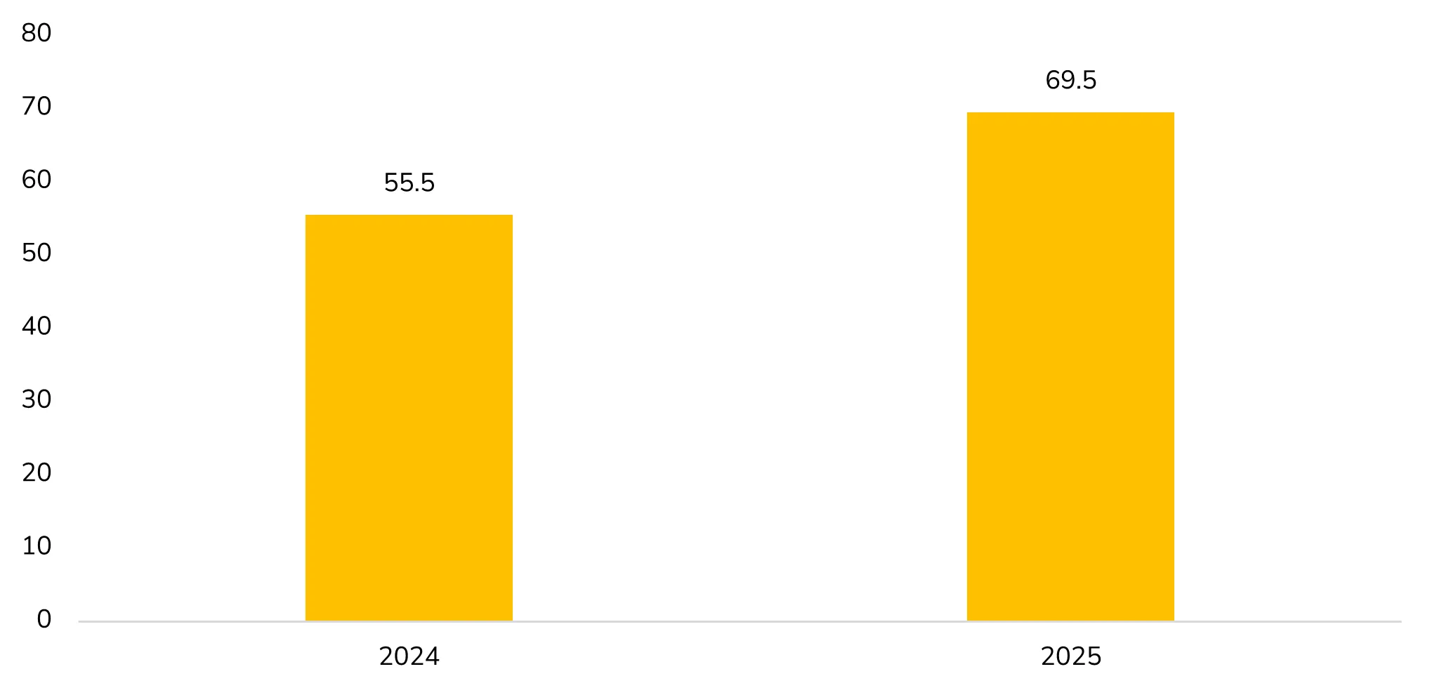 Source: The Semiconductor Industry Association (SIA)
Strategic Importance of Semiconductor Materials
It is no longer the case that semiconductor materials are just the basic inputs; they have become the strategic enablers. As the scaling of traditional transistors is slowing down, the progress of the semiconductor industry is increasingly dependent on breakthroughs in materials engineering rather than just on lithographic advancements. Materials largely determine circuit density, thermal performance, power efficiency, and even the device lifetime. The move towards 3D architectures, chiplet-based designs, gate-all-around transistors, EUV lithography, and heterogeneous integration has affected the materials systems in terms of their complexity and the level of detail largely required. High-bandwidth memory, AI accelerators, and automotive power semiconductors, for example, each require highly specialized materials suites that differ greatly from those used in conventional consumer electronics. Besides that, semiconductor fabrication goes through over one thousand different process steps, where each step requires extremely pure chemicals, gases, metals, or specially made substrates. If there is any contamination, variation in the formula, or inconsistency in the deposition, it can ruin device output worth billions of dollars. Hence, materials suppliers are extensively involved in the process development cycles at big foundries like TSMC, Samsung, Intel, Micron, SK Hynix, and Kioxia. Their role is not only important in leading-edge nodes but also in making mature nodes scalable, which can be used for automotive, industrial, and IoT market segments that, when combined, are among the fastest-growing demand clusters globally. Applied Materials, Inc. had a range of new systems for the fabrication of semiconductors that help the performance of advanced logic and memory chips, which are the basis of AI computing. Their new offerings go after those three areas that matter most in the contest to come up with AI chips of even greater power: leading-edge logic with GAA (Gate-All-Around) transistors, high-performance DRAM, e.g. high-bandwidth memory (HBM), and advanced packaging for the production of highly integrated systems-in-a-package which, in turn, allow for the optimization of chip performance, power consumption as well as cost.Leadership in the Wafer Substrate Segment
At the center of the entire semiconductor supply chain are silicon wafers, literally the ground on which the industry stands, and power in this sector is very tightly held by a handful of companies. These companies from Japan, Taiwan, and Europe are in the lead because of their long-term accumulated expertise in crystal growth, wafer polishing, and process purity. Shin-Etsu Chemical and Sumco, both of Japan, are generally considered the global leaders going together, they control most of the world market of high-purity silicon wafers. Their supremacy is due to thorough R&D investment, excellent process stability, and their capability to provide ultra-flat, defect-free wafers of increasing diameters, such as 300mm and the new 450mm standard that is still being evaluated for the next manufacturing nodes. After a very short period, GlobalWafers, a company based in Taiwan, has gone out of hand and is now a critical instrument in providing wafers for leading-edge as well as specialty areas. The changes it made to the way it does acquisitions, the upgrade of its technologies, and the worldwide location of its production have been the main factors that have its confrontational position. The European wafer producer Siltronic is also very important, mostly in the case of wafer polishing, where advanced and engineered substrates that are used for high-voltage and power devices are made. The Korean companies like SK Siltron are the ones who are mainly driving the progress in silicon carbide (SiC) wafers for high-power EV, industrial, and renewable energy systems. With the world's movement towards the use of electric vehicles and advanced computing, SiC and GaN substrates are the key materials, and the companies that have know-how in these engineered materials will be the ones that will have the strategic advantage.Advanced Chemicals
Where wafers are the structural basis of chipmaking, semiconductor chemicals are the vital and very intricate means by which each layer is shaped, etched, and perfected. These are the products that include photoresists, etchants, developers, cleaning agents, CMP slurries, dielectric coatings, and high-purity solvents. This is a domain that is mainly dominated by Japanese, American, and South Korean companies, with each of them delivering ultra-refined materials with purity levels that most of the time are beyond parts-per-trillion. JSR, Tokyo Ohka Kogyo (TOK), and Shin-Etsu Chemical are still the top three companies in photoresists that have significant control over the global lithography materials market. Their partnership with ASML and big foundries has been a major factor in the creation of materials that can be used with EUV lithography, which is a very important requirement for process technologies of the future. Other companies like Dow Chemical and DuPont are also very influential in the supply of advanced dielectric materials, CMP (chemical-mechanical planarization) solutions, and specialty polymers that are used for insulating layers and interconnect architectures. Cleanroom chemical suppliers in South Korea have been the focus of attention in the last couple of years. Notably, ENF Technology and Soulbrain have been acknowledged as the primary sources of high-purity electronic-grade chemicals, especially in the cleaning and etching areas, which are the most common steps in wafer processing. On the other hand, several Taiwanese companies are taking advantage of the closeness of TSMC and UMC to supply large-volume chemical raw materials that are ideal for cutting-edge technological processes. With the progression of lithography techniques and the decrease of transistor dimensions, the complexity of chemical formulations keeps increasing, which ultimately results in suppliers having to come up with innovations at a much quicker pace than before.Specialty Gases
Plasma etching, deposition processes, doping, and chamber cleaning are some of the applications where semiconductor manufacturing makes extensive use of specialty gases. These gases are mainly supplied by global industrial gas giants such as Linde, Air Liquide, and Air Products, who are the leaders in this segment. They have numerous purification and distribution systems that can meet semiconductor-grade standards and are spread over a vast area. Specialty gases such as nitrogen trifluoride, argon, xenon, neon, and high-purity hydrogen are necessary to keep process stability in EUV lithography and advanced plasma tools. The availability of neon, especially, has become a matter of geopolitical concern, and variations in worldwide supply chains have led fabs to diversify their sources and implement recycling systems. These gas providers are not just transport companies; they are technology partners who deliver ultrapure formulations, stable quality, and a continuous supply, an extremely important condition for high-volume fabs running 24/7 continuous cycles. Concretely, the major Asian players SK Materials, Versum, and Hyosung compete strongly in a few specific gas segments, which are mainly the gases used in the deposition and etching processes. Their closeness to fabs in South Korea and Taiwan guarantees the quick implementation of new recipes and makes them very compatible with the continuous changes of process nodes.Packaging Materials
The delineated segment is essentially supported by a chain of essential materials such as underfill compounds, bonding wires, encapsulation materials, redistribution layers, advanced substrates, solders, and thermal interface materials. For instance, Ajinomoto Fine-Techno, which is prominently recognized for its Ajinomoto Build-up Film (ABF), is virtually a monopolist in certain high-performance substrate materials that find usage in GPUs, AI accelerators, and server processors. The supremacy of this has resulted in the scarcity of supplies in times of increased demand, which is notably the case during the AI and cloud computing boom. Significant substrate producers such as Ibiden, Shinko Electric, Unimicron, Nan Ya PCB, and SEMCO are very important in the creation of high-density packaging substrates that are the basis for multi-chip organization and high-speed interconnects. The debut of 3D packaging technologies has, in fact, doubled the demand for highly engineered materials that provide thermal reliability, mechanical stability, and ultra-low signal interference. On the one hand, Heraeus and Tanaka, as suppliers of bonding wires, lead the fine-pitch gold and copper wire segment; on the other hand, companies dealing with thermal materials, e.g., Henkel and Lord Corporation, are very important in the process of heat dissipation for high-power devices.The Impact of Technology Megatrends on Materials Demand
Several major trends are reshaping the demand dynamics across the semiconductor materials landscape: 1. AI and High-Performance Computing AI accelerators, GPUs, and data-center processors need advanced photoresists, high-power substrates, and packaging materials that can handle extreme current densities and heat loads. The explosion of AI workloads has therefore caused the demand for ABF substrates, high-density interconnects, and advanced thermal materials to skyrocket. 2. Automotive Electrification and Autonomous Systems Power semiconductors such as SiC and GaN devices are the main components that make electric vehicles, charging infrastructure, and ADAS systems work. This transformation has elevated the role of specialty substrates, high-power die attach materials, and solid encapsulation technologies. 3. 5G, Edge Computing, and IoT These segments are the main drivers of demand for RF materials, chemical vapor deposition films, low-k dielectrics, and advanced packaging solutions that are optimized for low latency and high-frequency performance. 4. Advanced Memory Technologies High-bandwidth memory, 3D NAND, and next-generation DRAM are extremely reliant on precision chemicals, advanced lithography materials, and engineered substrates that are made for very high thermal stability. 5. Sustainability and Green Manufacturing Pressures Environmental regulations and clean manufacturing initiatives are demanding that suppliers to provide eco-friendly solvents, recyclable materials, low-waste formulations, and energy-efficient production methods.Regional Landscape
The industry of semiconductor materials has been limited to a few locations due to various reasons of history, structural, and technological reasons. In the area of specialty chemicals, photoresists, silicon wafers, and high-purity materials, Japan is still a global leader without any serious rival. The whole environment of Japan, which is very hard to replicate, has been formed through a couple of decades of early investments, thorough precision manufacturing know-how, and the strong and easy links with the equipment suppliers. By and large, Taiwan and South Korea are the leaders when it comes to the development of materials related to advanced memory, logic manufacturing, and packaging technologies. The close location to the cutting-edge foundries TSMC, UMC, Samsung, SK Hynix allows them to have very quick iteration and co-development cycles. Through big global companies as well as small, specialized suppliers, the USA is still a major player in advanced polymers, CMP slurries, dielectric materials, deposition chemicals, and industrial gases. Europe is a major contributor to the production of the a.o. engineered substrates, specialty gases, and advanced wafer technologies, especially through enterprises in Germany and France. China is determined to become a major player in the global semiconductor industry. Part of that involves ramping up its local production of semiconductor materials, which is in line with self-sufficiency strategies that are aimed at promoting national pride over Chinese technology. Though the country is yet to fully get rid of the need for importation of cutting-edge materials, China is making a lot of strides in CMP slurries, cleaning chemicals, photoresists, and packaging substrates. China's importance in the global materials landscape will be very significant by the time the next decade rolls around. Semiconductor Materials and Applications Table| Semiconductor Material | Key Applications |
| Silicon (Si) | Microprocessors, memory chips, power electronics, sensors |
| Silicon Carbide (SiC) | Electric vehicles (EV inverters), power modules, and high-temperature devices |
| Gallium Nitride (GaN) | RF devices, 5G base stations, fast chargers, and radar systems |
| Germanium (Ge) | High-speed transistors, optoelectronics, and solar cells |
| Gallium Arsenide (GaAs) | LEDs, laser diodes, and high-frequency amplifiers |
| Indium Phosphide (InP) | Photonic devices, fiber-optic communication, and high-speed circuits |
| Quartz (SiO?) | Photomasks, wafer processing equipment, etching systems |
| Photoresists (DUV/EUV) | Lithography patterning in chip fabrication |
| Copper (Cu) | Interconnects in advanced ICs |
Outlook for the Next Decade
In the following decade, semiconductor materials are going to be the major factor that determines the direction of world technology in a much greater manner. The focus will be increasingly on the materials that make it possible:- sub-2nm lithography
- 3D stacked architectures
- chiplet-based integration
- high-power, wide-bandgap devices
- AI-optimized packaging
- sustainable, low-emission manufacturing
Conclusion
The worldwide semiconductor materials business is about to wheeler one of its most significant eras in history. Suppliers of materials have turned out to be the key facilitators of technology and strategic competitiveness due to the rapidly increasing demand for advanced chips and the ever more complicated process nodes. Their innovations determine the speed of semiconductor progress, have an impact on the stability of the global supply chain, and facilitate the development of leading technologies in AI, automotive, communication, and computing fields. The companies that have supremacy in this field are those because of their unmatched expertise in purity, precision, and co-development, strong relationships with the leading foundries of the world, and the capability to innovate at the atomic level.Get in Touch
Interested in this topic? Contact our analysts for more details.
Related Insights

How Teletherapy is Transforming Mental Healthcare in America
Jun 23, 2026
How Digital Health Records Improve Patient Care in the United States
Jun 22, 2026
Why the U.S. Is Seeing a Surge in Mental Health Care Needs
Jun 15, 2026
Top 10 Crude Oil Reserves in the World: How Iran–U.S. Tensions Are Reshaping Global Energy Markets
Jun 12, 2026
Top 10 Generative AI Companies in 2026: Products, Pricing, Funding, and Competitive Analysis
Jun 10, 2026