
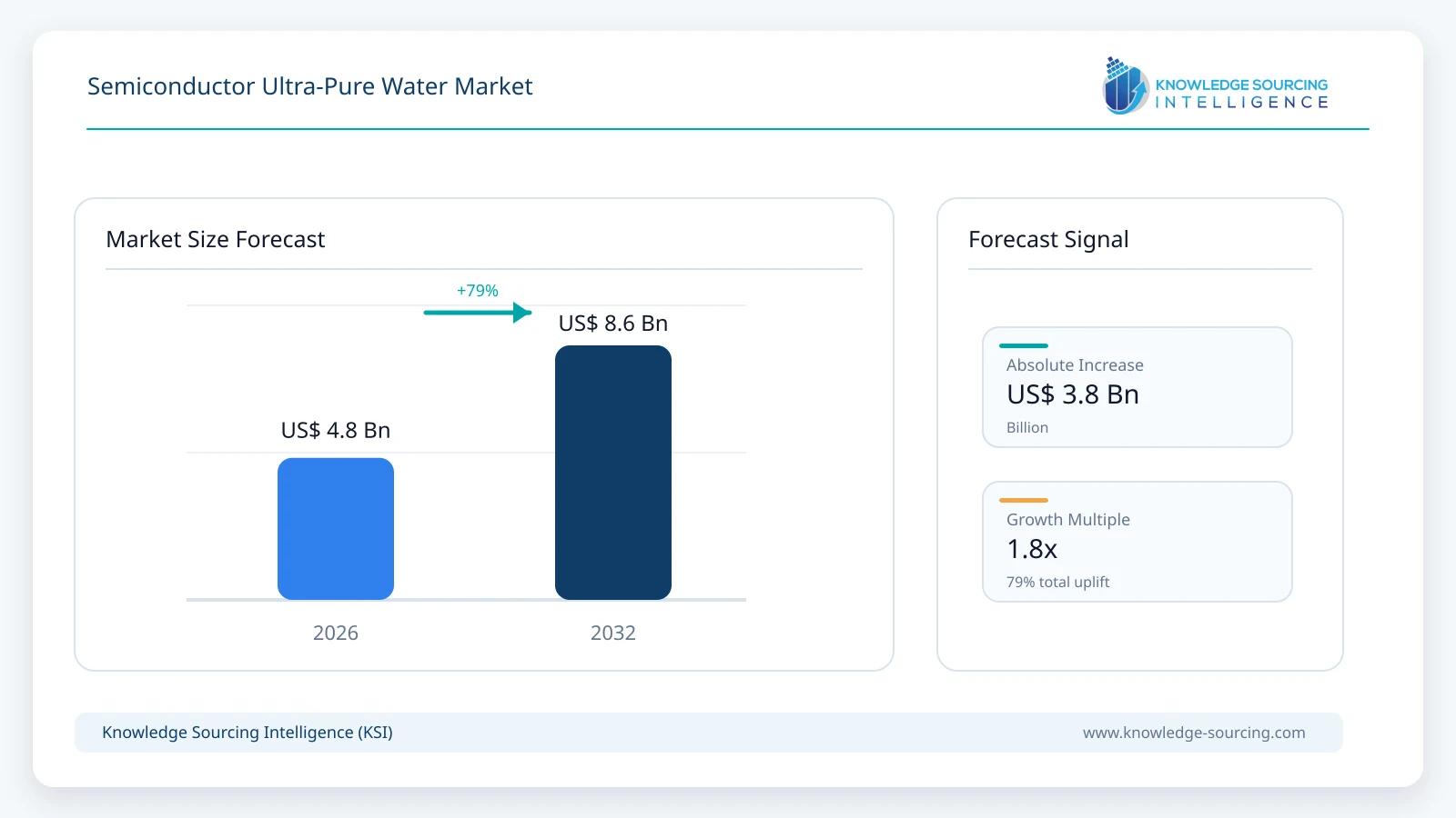
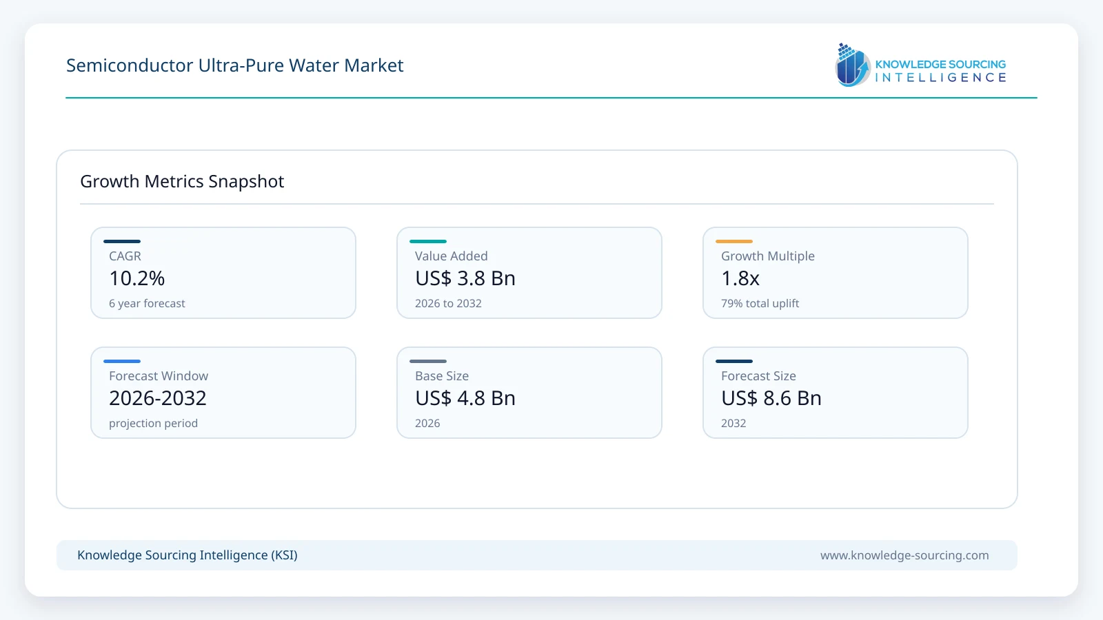
The Semiconductor Ultra-Pure Water Market is estimated at USD 4.80 billion in 2026 and is projected to reach USD 8.60 billion by 2032, representing a CAGR of 10.2% during 2026-2032.
Highlights:
- 1Front-end purification and final polishing remain the core UPW revenue pool in semiconductor fabs.
- 2Advanced logic and memory nodes increase UPW intensity because wafer cleaning steps multiply across longer process flows.
- 3Water reuse is moving closer to the UPW loop as fabs seek lower raw-water withdrawal and greater operating resilience.
- 4Online monitoring, low total-organic-carbon performance and particle control become more important as defect tolerances tighten.
- 5Asia Pacific remains the largest market because Taiwan, South Korea, Japan, China and Singapore contain dense clusters of high-volume fabs.
Market Overview
Semiconductor UPW plants convert incoming municipal, industrial or reclaimed feedwater into water that can be used directly on wafer surfaces without introducing yield-limiting contamination. A typical architecture begins with pretreatment to remove suspended solids, hardness and oxidants. Reverse osmosis removes most dissolved salts and organics, followed by ion-exchange or electrodeionization steps that drive ionic contamination lower. Ultraviolet oxidation reduces total organic carbon, membrane contactors remove dissolved gases, and ultrafiltration controls fine particles and microbial fragments. Final polishing loops then maintain water quality close to the point of use and continuously circulate water through high-purity distribution piping.
The purity requirement is extreme. Veolia describes ultrapure water as having resistivity around 18.2 MOhm-cm with very low total organic carbon and microbiological contamination. Samsung notes that UPW is used before and after multiple semiconductor process steps, including etching, ion implantation, polishing and wafer cutting, because even microscopic residual contamination can cause critical defects. For advanced fabs, the relevant purchasing question is therefore not only how much water a plant can produce, but whether the entire treatment and distribution chain can maintain stable ionic, organic, particle and dissolved-gas specifications under rapidly changing fab demand.
The market is also shifting from linear water use toward circular water architecture. Recovered rinse water can be segregated by quality and returned to lower-grade uses such as cooling towers, scrubbers or facility utilities, while higher-quality streams can undergo additional treatment for reintegration into process-water or UPW production. Samsung reported 78.8 million tonnes of ultrapure-water supply and 25.2 million tonnes of UPW recovery in 2025 across its operations. Micron states that ultrapure water is used for wafer cleaning and is increasingly linked with reclamation systems that reduce dependence on municipal water supplies. This integration expands the addressable market from standalone UPW production into recovery, monitoring and reuse engineering.
Market Drivers
Advanced nodes increase the number and sensitivity of wafer-cleaning steps
Shrinking geometries and increasingly complex device structures require more deposition, etch, implant, chemical-mechanical-polishing and cleaning cycles. Each additional wet clean or rinse step creates another point where ionic, organic or particle contamination can affect device yield. Samsung explicitly identifies UPW as the principal cleaning medium before and after many core semiconductor processes. As logic and memory manufacturing moves toward gate-all-around transistors, higher layer counts and more complex 3D structures, fabs require both higher UPW volumes and more stable control of contaminants at extremely low concentrations.
Global fab construction creates large greenfield UPW system opportunities
New semiconductor capacity in the United States, Japan, Taiwan, South Korea, Europe, India and Southeast Asia requires dedicated high-purity water infrastructure before process tools can enter production. TSMC Arizona is staffing facilities teams responsible for UPW, process cooling water and industrial-waste systems as its second and third fabs move toward production between 2028 and 2030. Micron is simultaneously building new water-recycling infrastructure for Boise and Gujarat and planning similar systems for New York. Every greenfield fab therefore creates an initial equipment opportunity followed by recurring service, membrane, resin, instrumentation and expansion demand.
Water scarcity and permitting pressure accelerate reuse integration
Semiconductor fabs are increasingly built in regions where water availability, drought risk or community scrutiny can constrain expansion. Intel targets net-positive water by 2030 and reported approximately 11.2 billion gallons of water conserved in 2025 through operations and collaborations. Samsung reduced water use through process optimization and reported large-scale internal reuse across Korean semiconductor sites. These targets encourage UPW suppliers to integrate reclamation, quality segregation and recovery controls into the fab water system rather than designing UPW plants as isolated once-through utilities.
Fab customers increasingly require full lifecycle service and water analytics
UPW performance depends on stable operation over many years. Membrane fouling, resin exhaustion, microbial control, total-organic-carbon excursions, particle release and distribution-loop contamination can disrupt wafer manufacturing even when nominal plant capacity is sufficient. Suppliers are therefore competing through remote monitoring, analytical services, predictive maintenance, chemical optimization and long-term operation contracts. Veolia, Kurita, Organo, Ovivo and other major suppliers increasingly position themselves across the complete semiconductor water cycle rather than only selling individual treatment skids.
Restraints and Adoption Challenges
The main constraint is the cost and complexity of achieving semiconductor-grade purity from increasingly variable feedwater. A system designed for one municipal source may require substantial modification if the fab increases recycled-water content or changes water sourcing. Higher recovery can also concentrate silica, hardness, organics and trace contaminants, raising pretreatment and membrane-management requirements. UPW plants consume energy, chemicals, membranes, resins and large volumes of flush water, so aggressive reuse targets can shift rather than eliminate operating costs. Fab operators must also maintain redundant treatment trains because a prolonged UPW quality excursion can stop production. Finally, qualification of new membranes, resins or treatment chemistries is conservative because any change that introduces trace contamination can create expensive yield losses.
Segment Analysis
By System Stage
Front-end purification and final polishing represent the central commercial categories because every fab requires bulk removal of dissolved contaminants followed by tightly controlled finishing steps. Pretreatment and reverse osmosis provide the first major purification barrier, while electrodeionization or ion exchange, ultraviolet oxidation, degassing and ultrafiltration drive water toward point-of-use specifications. Distribution and monitoring systems are becoming more valuable as fabs require continuous verification of resistivity, total organic carbon, particles and dissolved gases across large campuses.
UPW recovery and reuse integration is expected to grow fastest from a smaller base. Leading fabs increasingly separate water streams by contamination profile, allowing lightly contaminated rinses to be recovered for treatment and reuse. This requires additional membranes, polishing, analytics and control logic rather than simply larger bulk UPW plants. The commercial opportunity therefore expands as fabs pursue higher recovery rates without allowing recycled-water variability to compromise wafer cleanliness.
UPW System Layer | Primary Function | Semiconductor Relevance |
Pretreatment and reverse osmosis | Remove particles, hardness, organics and most dissolved salts | Protect downstream polishing systems and stabilize feed quality |
Ion removal and polishing | Reduce ionic contamination to ultra-low levels | Supports high resistivity and low trace-metal contamination |
UV oxidation and degassing | Reduce TOC and dissolved gases | Controls organic residues and gas-related process variability |
Ultrafiltration and final filtration | Remove fine particles and microbial fragments | Limits wafer-surface defects during cleaning and rinse steps |
Distribution and online monitoring | Maintain purity through circulating fab loops | Prevents contamination between central plant and process tools |
Recovery and reuse integration | Treat selected return streams for internal reuse | Reduces raw-water withdrawal and improves water resilience |
Market and Technology Indicators
Indicator | Current Evidence | Market Impact |
Microelectronics water bookings | Veolia reported EUR 343 million of bookings through July 2026, including semiconductor projects in Singapore and the United States. | Shows large greenfield and expansion demand for integrated UPW and reclamation systems. |
UPW recovery at scale | Samsung reported 78.8 million tonnes of UPW supply and 25.2 million tonnes recovered in 2025. | Demonstrates that recovery is becoming a material part of fab water architecture. |
India semiconductor build-out | Kurita Membrane India highlighted UPW production and semiconductor water-analysis capabilities at SEMICON India 2026. | Creates a new regional supplier base around upcoming fabs and packaging plants. |
Memory-fab water investment | Micron is building water-reuse infrastructure in Boise and Gujarat and planning similar facilities for New York. | Links new memory capacity with higher spending on water recovery and UPW integration. |
Advanced U.S. fab expansion | TSMC Arizona facilities roles explicitly cover UPW, PCW and industrial-waste systems as additional fabs move toward production. | Supports recurring equipment, commissioning and lifecycle-service demand. |
Water stewardship targets | Intel targets net-positive water by 2030 and reported major conservation and restoration progress in 2025. | Raises demand for higher-recovery systems and water-loop optimization. |
Regional Opportunity
Asia Pacific
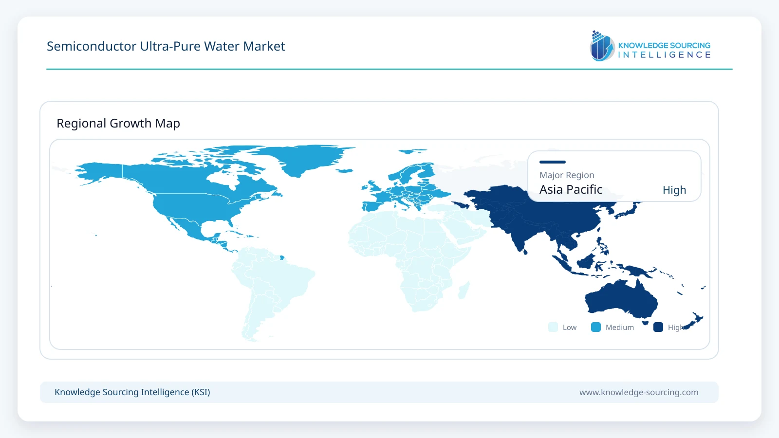
Asia Pacific is the largest semiconductor UPW market because it combines the highest concentration of wafer fabrication capacity with a mature regional water-treatment supplier base. Taiwan, South Korea and Japan host large advanced logic and memory fabs that operate extensive UPW plants continuously, while China and Singapore add high-volume foundry, memory and specialty-semiconductor demand. New fabs in India and Southeast Asia broaden the opportunity beyond the established Northeast Asian clusters.
Japan is particularly important on the supplier side. Organo, Kurita Water Industries and Nomura Micro Science have long semiconductor-water experience and provide design, equipment, chemicals, monitoring and service capabilities. Kurita states that water-resource limitations and the standardization of ultrapure-water requirements are becoming more important as semiconductor production expands. Its 2026 India joint venture also illustrates how Japanese water expertise is being exported into emerging semiconductor geographies.
South Korea provides one of the clearest examples of water intensity and recovery operating at very large scale. Samsung reported 78.8 million tonnes of UPW supply in 2025 and more than 25 million tonnes of recovery, while its semiconductor division continues to track reuse rates by water category and site. Taiwan has similarly large requirements around leading-edge logic, foundry and advanced packaging, where water quality must remain stable across growing campuses. Singapore combines major semiconductor production with explicit emphasis on reclaimed-water supply and zero-liquid-discharge approaches, including the projects cited by Veolia during 2026.
North America is the fastest strategic expansion region as TSMC, Intel, Micron and other manufacturers add leading-edge capacity in Arizona, Idaho, New York and additional U.S. locations. These greenfield projects create high-value opportunities because UPW plants must be installed before process qualification begins. Europe contributes through logic, power semiconductor and specialty fabs, while water scarcity and permitting constraints encourage higher reuse. India remains an early-stage but increasingly important opportunity as domestic semiconductor projects create demand for local UPW engineering, membranes, service and analytical capability.
Competitive Landscape
The competitive landscape combines integrated semiconductor-water engineering companies, membrane and purification specialists, analytical-instrument providers and local EPC/service partners. Organo, Kurita Water Industries, Veolia Water Technologies, Ovivo and Nomura Micro Science are prominent integrated suppliers. Xylem through its Evoqua heritage participates in high-purity water and ion-treatment systems, while Ecolab, DuPont Water Solutions, Toray Industries, Asahi Kasei and other material suppliers contribute membranes, resins, chemicals and process technologies used within UPW plants.
Differentiation depends on more than nominal flow capacity. Semiconductor customers evaluate particle performance, total organic carbon, resistivity stability, dissolved oxygen, trace metals, microbial control, uptime, recovery ratio, chemical consumption and the ability to maintain water quality over long distribution loops. Suppliers with installed-base service teams and analytical capability have an advantage because fabs require rapid response to excursions and ongoing optimization over the full asset life.
The market is gradually consolidating around full water-cycle capability. Fab customers increasingly prefer suppliers that can connect UPW generation with wastewater segregation, reclamation, zero-liquid-discharge design and water-reuse targets. Veolia’s 2026 bookings and Kurita’s semiconductor expansion illustrate this shift. However, specialized membrane, resin and monitoring suppliers remain important because the highest-purity stages often require proprietary materials and instrumentation that integrated EPC providers source from technology partners.
Major companies and ecosystem participants covered: Organo Corporation, Kurita Water Industries, Veolia Water Technologies, Ovivo, Nomura Micro Science, Xylem / Evoqua, Ecolab, DuPont Water Solutions, Toray Industries, Asahi Kasei, Pall Corporation, Gradiant, Aquatech, Pentair, Meiden Engineering and regional semiconductor-water EPC specialists.
Recent Developments
July 2026: Veolia Water Technologies reported EUR 343 million in microelectronics water-technology bookings since the start of the year, including semiconductor projects in Singapore and the United States covering ultrapure-water production and advanced water reclamation.
September 2026: Kurita Membrane India showcased ultrapure-water production, wastewater reclamation, resource-recovery and semiconductor water-analysis capabilities at SEMICON India 2026.
June 2026: Kurita Water Industries and Membrane Group established Kurita Membrane India to serve the expanding semiconductor industry in India.
2026: Micron reported ongoing construction of advanced water recycling and reuse facilities in Boise and Gujarat and plans for similar systems as part of its New York expansion.
2026: Samsung reported continued expansion of semiconductor water reuse, with 2025 ultrapure-water supply of 78.8 million tonnes and recovery of 25.2 million tonnes.
2026: TSMC Arizona expanded facilities staffing for ultrapure-water, process-cooling-water and industrial-waste systems as additional advanced fabs move toward production.
Semiconductor Ultra-Pure Water Market Scope:
| Report Metric | Details |
|---|---|
| Total Market Size in 2026 | USD 4.80 billion |
| Total Market Size in 2032 | USD 8.60 billion |
| Forecast Unit | Billion |
| Growth Rate | 10.2% |
| Study Period | 2021 to 2032 |
| Historical Data | 2021 to 2024 |
| Base Year | 2025 |
| Forecast Period | 2026 – 2032 |
| Segmentation | System Stage, Fab Application, Service Model, Geography |
| Companies |
|
Market Segmentation
By System Stage
Pretreatment
Reverse Osmosis
Electrodeionization and Ion Exchange
UV Oxidation and TOC Control
Membrane Degassing
Ultrafiltration and Final Polishing
Distribution and Online Monitoring
Recovery and Reuse Integration
By Fab Application
Wafer Cleaning and Rinsing
Chemical Mechanical Planarization
Wet Etch and Surface Preparation
Implant and Deposition Process Support
Advanced Packaging and Wafer-Level Processing
Research and Specialty Semiconductor Fabs
By Service Model
Greenfield UPW System Engineering
Brownfield Expansion and Retrofit
Operations and Maintenance
Membranes, Resins and Consumables
Monitoring and Analytical Services
By Geography
Asia Pacific
Taiwan
South Korea
Japan
China
Singapore and Southeast Asia
India
North America
Europe
Rest of World
Table of Contents
1. EXECUTIVE SUMMARY
1.1. Market Opportunity and Key Findings
1.2. Semiconductor UPW Demand Outlook
1.3. Principal Revenue Pools
2. MARKET OVERVIEW
2.1. Semiconductor UPW Quality Requirements
2.2. Feedwater Pretreatment Architecture
2.3. Reverse Osmosis and Ion Removal
2.4. TOC Reduction, Degassing and Final Polishing
2.5. Distribution Loops and Point-of-Use Control
2.6. UPW Recovery and Reuse Integration
3. MARKET SIZE AND FORECAST, 2026-2032
3.1. Global Market Revenue
3.2. Annual Growth Analysis
3.3. Fab Water Intensity and System-Capacity Drivers
4. MARKET BY SYSTEM STAGE
4.1. Pretreatment
4.2. Reverse Osmosis
4.3. Electrodeionization and Ion Exchange
4.4. UV Oxidation and TOC Control
4.5. Membrane Degassing
4.6. Ultrafiltration and Final Polishing
4.7. Distribution and Online Monitoring
4.8. Recovery and Reuse Integration
5. MARKET BY FAB APPLICATION
5.1. Wafer Cleaning and Rinsing
5.2. Chemical Mechanical Planarization
5.3. Wet Etch and Surface Preparation
5.4. Implant and Deposition Process Support
5.5. Advanced Packaging and Wafer-Level Processing
5.6. Research and Specialty Semiconductor Fabs
6. MARKET BY SERVICE MODEL
6.1. Greenfield UPW System Engineering
6.2. Brownfield Expansion and Retrofit
6.3. Operations and Maintenance
6.4. Membranes, Resins and Consumables
6.5. Monitoring and Analytical Services
7. REGIONAL MARKET
7.1. Asia Pacific
7.1.1. Taiwan
7.1.2. South Korea
7.1.3. Japan
7.1.4. China
7.1.5. Singapore and Southeast Asia
7.1.6. India
7.2. North America
7.3. Europe
7.4. Rest of World
8. MARKET DYNAMICS
8.1. Drivers
8.1.1. Advanced-Node Wafer-Cleaning Intensity
8.1.2. Global Fab Construction
8.1.3. Water Scarcity and Reuse Targets
8.1.4. Lifecycle Service and Monitoring Demand
8.2. Restraints
8.2.1. High Capital and Redundancy Requirements
8.2.2. Variable Feedwater and Recycled-Water Quality
8.2.3. Energy, Chemical and Consumable Intensity
8.2.4. Conservative Qualification of New Materials
9. COMPETITIVE LANDSCAPE
9.1. Market Structure and Competitive Intensity
9.2. Integrated UPW System Suppliers
9.3. Membrane, Resin and Purification Technologies
9.4. Monitoring and Analytical Platforms
9.5. Reuse and Full Water-Cycle Strategies
10. COMPANY PROFILES
10.1. Organo Corporation
10.2. Kurita Water Industries
10.3. Veolia Water Technologies
10.4. Ovivo
10.5. Nomura Micro Science
10.6. Xylem / Evoqua
10.7. Ecolab
10.8. DuPont Water Solutions
10.9. Toray Industries
10.10. Asahi Kasei
10.10. Pall Corporation
10.12. Gradiant
10.13. Aquatech
10.14. Pentair
10.15. Meiden Engineering
11. RECENT DEVELOPMENTS
12. Appendix
Navigate
Trusted by the world's leading organizations











