
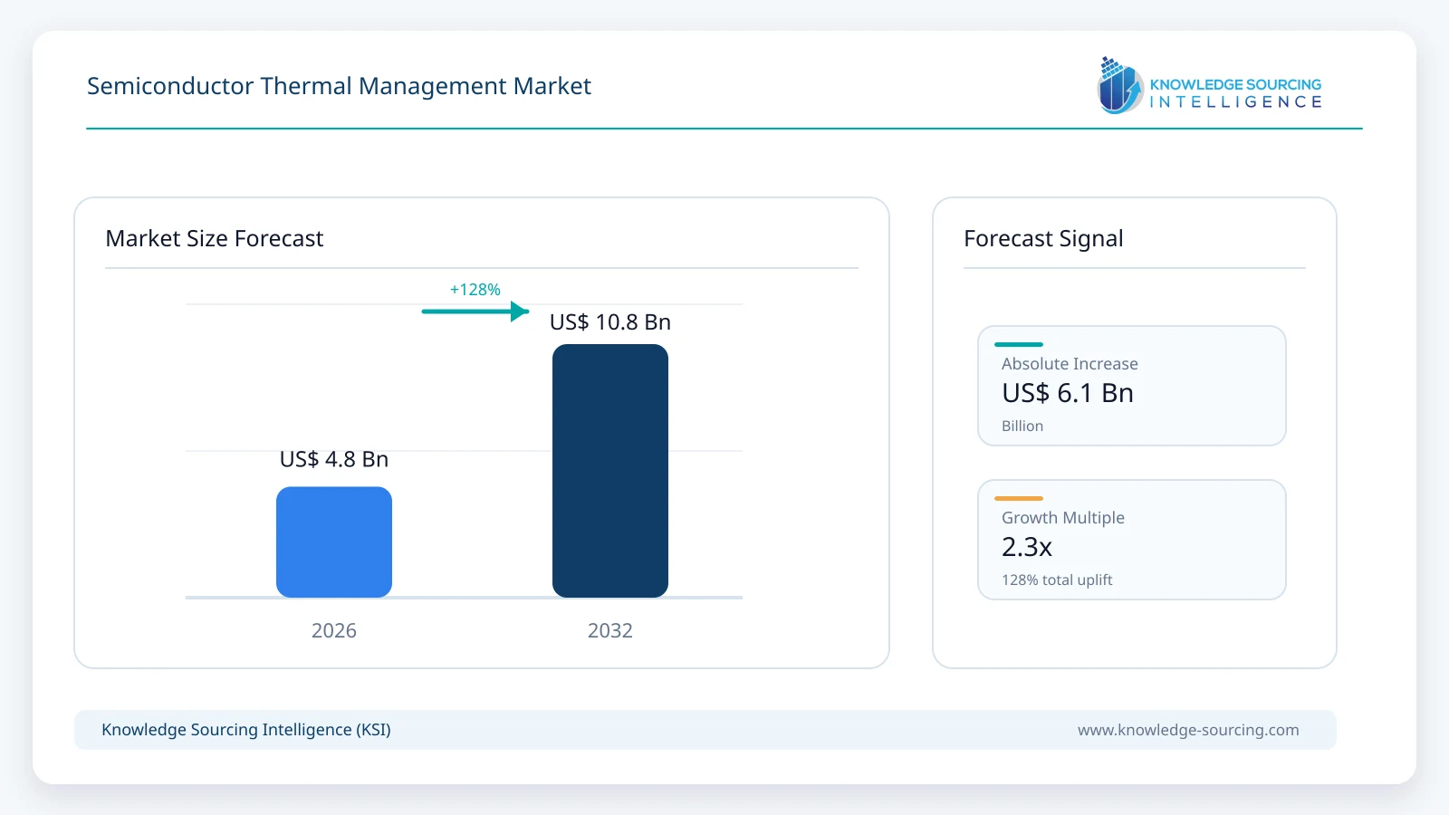
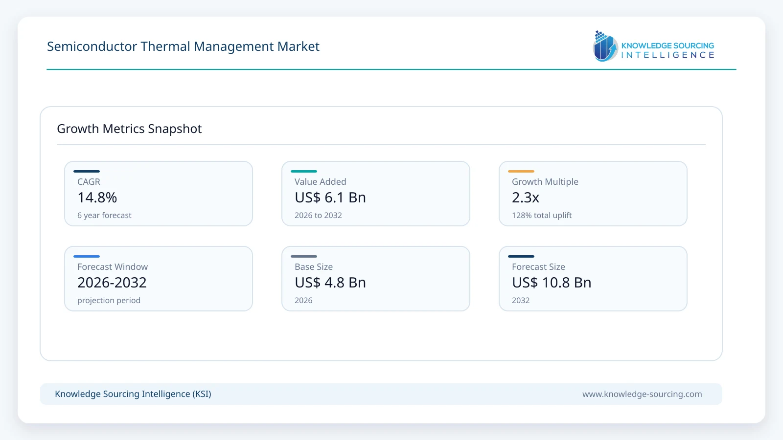
The Semiconductor Thermal Management Market is estimated at USD 4.75 billion in 2026 and is projected to reach USD 10.85 billion by 2032, representing a CAGR of 14.8% over 2026-2032.
Highlights:
- 1Thermal interface materials remain the largest 2026 revenue pool across semiconductor package cooling.
- 2Metal and phase-change interfaces grow faster as AI package heat flux exceeds polymer-only solutions.
- 3Integrated heat spreaders and package lids remain essential for controlling hotspot and warpage behavior.
- 4AI accelerators, HBM and power semiconductors are the strongest premium thermal-management demand sources.
- 5Package-integrated two-phase and vapor-spreading structures emerge fastest from a small commercial base.
The thermal path inside a semiconductor package usually begins at the active die, passes through a first thermal interface, reaches an integrated heat spreader or lid and then transfers into a system-level cooler. Every interface adds thermal resistance. As AI and high-performance computing packages become larger and combine several logic and memory dies, heat distribution becomes less uniform and package warpage makes maintaining a thin, repeatable bond line more difficult. The commercial value therefore moves toward materials and structures that combine high thermal conductivity with low mechanical stress, stable contact and long-term reliability.
TIM1 sits between the semiconductor die and lid or integrated heat spreader and is one of the most demanding thermal interfaces because it operates close to the heat source. TIM1.5 applies to selected bare-die or package architectures between the die and a heat-spreading structure. Polymer TIMs remain widely used because they are compliant and manufacturable, while indium, solder and other metal interfaces gain relevance where higher heat flux justifies more complex assembly. Honeywell identifies TIM1.5 as increasingly important for high-performance processors, while Indium Corporation is developing metal TIM solutions specifically for large AI packages.
Heat spreading is also evolving. Copper lids remain standard across many processors, but graphite structures, composite spreaders and two-phase devices can reduce local hotspot intensity. Boyd supplies ultra-thin vapor chambers, heat pipes and CTE-matched spreaders for high-heat-flux electronics, while package designers increasingly evaluate lid geometry, stiffener design and TIM behavior together. The result is a thermal-management market that is closely tied to semiconductor packaging rather than only to external cooling hardware.
Market Drivers
AI accelerators are increasing package heat flux
Large AI processors combine high power with very large package areas and dense memory integration. Higher package power raises the value of every reduction in thermal resistance because lower junction temperature can preserve frequency, reliability and accelerator utilization. Henkel identifies thermal dissipation and package warpage as central material challenges for large AI and HPC packages, while Indium is developing metal TIM approaches for high-TDP xPU packages. This directly increases spending on premium TIMs, spreaders and package-level thermal structures.
Advanced packaging concentrates heat across multi-die assemblies
2.5D and 3D packaging can place logic chiplets and HBM stacks in close proximity, creating multiple heat sources with different power densities. A single lid or heat spreader must distribute those loads without creating excessive temperature gradients or mechanical stress. The problem becomes harder as package size expands. Thermal management therefore becomes part of package architecture, affecting lid design, material selection, interface thickness and die placement before assembly begins.
Power semiconductors require electrically and thermally robust interfaces
Silicon carbide, gallium nitride and high-current silicon devices can operate at elevated junction temperatures and high power density. Thermal-interface materials must transfer heat while maintaining dielectric strength, electrical isolation where required and reliability under repeated temperature cycling. Parker Chomerics explicitly positions high-conductivity pads and thin-bond-line gels for power semiconductors, memory modules and processors. Electrification therefore broadens thermal-management demand beyond computing.
Higher-volume automated assembly favors dispensable and pre-engineered materials
Manual application becomes less attractive as advanced packages move into higher volumes. Dispensable thermal gels, phase-change films and preformed interfaces can improve repeatability and reduce assembly variation. Parker Chomerics is expanding one-part dispensable gels and higher-conductivity pads, while Henkel emphasizes automated application and package-level material integration. Manufacturing compatibility therefore becomes nearly as important as bulk thermal conductivity.
Restraints and Adoption Challenges
The market is constrained by the trade-off between thermal conductivity, mechanical compliance, pump-out resistance, electrical isolation and manufacturability. Highly conductive metal interfaces can create assembly and rework challenges, while softer polymer materials may introduce higher thermal resistance. Large packages can warp during thermal cycling, changing bond-line thickness and contact pressure. New graphite, vapor-chamber and composite structures must also fit package-height and reliability requirements. In addition, some thermal-management value can shift outside the package as data centers adopt direct liquid cooling, meaning package-level thermal improvements and system-level cooling increasingly have to be optimized together.
Semiconductor Thermal Management Market Segment Analysis
By Thermal Management Product
Thermal interface materials represent the largest revenue contribution in 2026 because nearly every high-power semiconductor package requires one or more engineered interfaces between the die, lid, spreader or external cooler. Premium metallic and phase-change interfaces contribute higher value per package in AI, HPC and power-electronics applications, while polymer gels, greases and films remain the largest-volume technologies.
Package-integrated vapor-spreading and two-phase structures are expected to grow fastest through 2032 from a smaller base. Their adoption increases where conventional lids and TIMs cannot spread localized heat flux effectively enough. Integrated heat spreaders and lids remain a substantial category, with increasing design complexity around CTE matching, warpage, surface flatness and multi-die hotspot distribution.
Thermal Management Category | Revenue Contribution | Growth Direction | Primary Semiconductor Application |
TIM1 / TIM1.5 materials | Largest | Strong | Die-to-lid and die-to-spreader heat transfer |
Integrated heat spreaders and lids | High | Strong | CPUs, GPUs, AI accelerators and large multi-die packages |
Metal and phase-change thermal interfaces | Growing | Very strong | High-TDP AI/HPC and premium processor packages |
Thermal adhesives and lid/stiffener materials | Established | Strong | Package flatness, lid attach and mechanical reliability |
Graphite and advanced heat-spreading structures | Growing | Very strong | Hotspot spreading in compact high-power packages |
Package-integrated vapor / two-phase structures | Emerging | Fastest | Extreme heat-flux AI, HPC and advanced power devices |
Market and Technology Indicators
Indicator | Revenue Contribution | Market Impact |
Metal TIM performance | Indium reported indium-based solder TIM thermal conductivity of about 86 W/mK for large AI/HPC packages. | Supports transition toward lower-resistance interfaces at very high TDP. |
Package-level AI thermal materials | Henkel identifies TIMs, lid/stiffener attach and warpage control as core AI advanced-packaging needs. | Links thermal management directly to package reliability and manufacturing. |
2026 TIM portfolio expansion | Parker Chomerics expanded thermal pads, gels, greases and thin-bond-line products during 2026. | Shows broad commercial investment across multiple interface formats. |
TIM1.5 adoption | Honeywell identifies TIM1.5 as increasingly relevant for high-performance AI processors and GPUs. | Expands demand for die-to-spreader and bare-die thermal interfaces. |
Two-phase spreading capability | Boyd commercializes ultra-thin vapor chambers, thermosiphons and advanced heat spreaders. | Provides a pathway beyond purely conductive package cooling. |
Advanced packaging demand | AI package expansion is increasing thermal, warpage and reliability requirements across foundry and OSAT ecosystems. | Raises thermal-management content per high-value semiconductor package. |
Regional Opportunity
Asia Pacific
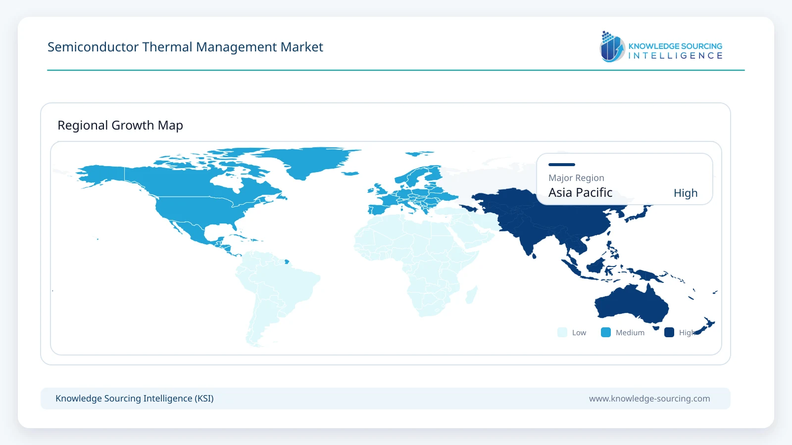
Asia Pacific is the largest market for semiconductor thermal management because the region contains the majority of semiconductor packaging, processor manufacturing, memory production and electronics assembly. Taiwan and South Korea are especially important through AI accelerator packaging, HBM and foundry capacity, while Japan supplies advanced thermal materials, graphite, adhesives and precision packaging technologies. China adds large power-semiconductor, server and electronics manufacturing demand.
The region's role in advanced packaging gives thermal suppliers direct access to package qualification programs. TSMC, ASE, Samsung and SK hynix increasingly work with materials and component suppliers during package development rather than after the semiconductor design is fixed. Large 2.5D packages require warpage control, lid attachment and low-resistance thermal interfaces to be qualified alongside interposer and substrate designs.
Japan remains important through Shin-Etsu Chemical, Panasonic Industry, Fujipoly and other materials suppliers, while Taiwan and South Korea combine customer scale with advanced packaging production. China is a major volume market for thermal materials used in processors, power semiconductors and communications hardware. Southeast Asia also gains relevance as advanced packaging and electronics manufacturing expands.
North America is the largest design and premium-demand region through AI processors, HPC systems and data-center hardware. Henkel, Indium, Parker Chomerics, Honeywell, Boyd and several advanced-materials suppliers have significant development activity in the region. Europe contributes through advanced materials, automotive power semiconductors and high-reliability industrial electronics.
Competitive Landscape
The competitive landscape combines semiconductor materials companies, thermal-interface specialists and engineered thermal-hardware suppliers. Henkel competes across package-level TIMs, lid/stiffener attach and advanced packaging materials. Indium Corporation is differentiated in metal and solder thermal interfaces, particularly for very high heat-flux processors. Parker Chomerics has a broad pad, gel, grease and phase-change portfolio, while Honeywell participates in high-performance phase-change and processor thermal interfaces.
Shin-Etsu Chemical, Fujipoly, Panasonic Industry, Qnity / Laird and Dow compete across silicone, polymer, gap-filler and specialty thermal-material platforms. Boyd extends competition into heat spreaders, vapor chambers, graphite structures and complete thermal assemblies. Momentive and Saint-Gobain also participate in high-performance interface and dielectric thermal materials.
Competitive differentiation increasingly depends on effective thermal impedance at the actual bond line, not bulk W/mK alone. Package designers evaluate pump-out, voiding, compression stress, reworkability, outgassing, CTE compatibility, reliability and automated dispensing. Vendors that can co-design the interface, lid and spreading structure with package engineers are better positioned as AI package thermal loads increase.
Major companies and ecosystem participants covered: Henkel, Indium Corporation, Parker Hannifin / Chomerics, Honeywell, Shin-Etsu Chemical, Qnity / Laird Performance Materials, Boyd, Fujipoly, Panasonic Industry, Dow, Momentive Performance Materials, Saint-Gobain, 3M, DuPont and T-Global Technology.
Recent Developments
August 2026: Indium Corporation highlighted high-performance TIM solutions for AI packaging and high-power semiconductor applications at SEMICON Taiwan.
July 2026: Indium Corporation presented metal thermal-interface solutions for large-area high-TDP AI and HPC packages at IMAPS ThermCon.
May 2026: Indium Corporation presented indium-based solder TIM research for large BGA and AI packages at IEEE ECTC.
2026: Parker Chomerics expanded its thermal-interface portfolio with new gap pads, gels, dispensable fillers and greases for next-generation electronics.
2026: Henkel expanded package-level AI thermal-management materials spanning TIMs, underfills and lid/stiffener attach solutions.
2026: Semiconductor packaging suppliers increased focus on thermal co-design as AI packages moved toward larger multi-die and HBM configurations.
Semiconductor Thermal Management Market Scope:
| Report Metric | Details |
|---|---|
| Total Market Size in 2026 | USD 4.75 billion |
| Total Market Size in 2032 | USD 10.85 billion |
| Forecast Unit | USD Billion |
| Growth Rate | 14.8% |
| Study Period | 2021 to 2032 |
| Historical Data | 2021 to 2024 |
| Base Year | 2025 |
| Forecast Period | 2026 – 2032 |
| Segmentation | Thermal Management Product, Material Platform, Semiconductor Type, Packaging Architecture, End User, Geography |
| Companies |
|
Market Segmentation
By Thermal Management Product
TIM1 and TIM1.5 Materials
Integrated Heat Spreaders and Lids
Metal and Phase-Change Thermal Interfaces
Thermal Adhesives and Lid/Stiffener Materials
Graphite and Advanced Heat-Spreading Structures
Package-Integrated Vapor and Two-Phase Structures
By Material Platform
Polymer and Silicone Interfaces
Metal and Solder Interfaces
Phase-Change Materials
Graphite and Carbon-Based Materials
Copper, Aluminum and Composite Spreaders
By Semiconductor Type
CPUs and GPUs
AI Accelerators and HPC Processors
HBM and Advanced Memory
Power Semiconductors
Networking and Optical Semiconductors
Automotive and Industrial ICs
By Packaging Architecture
Flip-Chip BGA
2.5D Interposer and Bridge Packages
3D and Hybrid-Bonded Packages
Power Modules
Wafer-Level and Fan-Out Packages
By End User
Data Centers and High-Performance Computing
Consumer Electronics
Automotive
Industrial and Power Electronics
Telecommunications
By Geography
Asia Pacific
Taiwan
South Korea
Japan
China
Southeast Asia and India
North America
Europe
Rest of World
Table of Contents
1. EXECUTIVE SUMMARY
1.1. Market Opportunity and Key Findings
1.2. Semiconductor Thermal-Density Outlook
1.3. Principal Revenue Pools
2. MARKET OVERVIEW
2.1. Package-Level Thermal Resistance Path
2.2. TIM1, TIM1.5 and Heat-Spreader Architecture
2.3. Integrated Heat Spreaders and Package Lids
2.4. Graphite, Metal and Two-Phase Heat Spreading
2.5. Thermal Co-Design with Advanced Packaging
3. MARKET SIZE AND FORECAST, 2026-2032
3.1. Global Market Revenue
3.2. Annual Growth Analysis
3.3. Thermal Content per Semiconductor Package
4. MARKET BY THERMAL MANAGEMENT PRODUCT
4.1. TIM1 and TIM1.5 Materials
4.2. Integrated Heat Spreaders and Lids
4.3. Metal and Phase-Change Thermal Interfaces
4.4. Thermal Adhesives and Lid/Stiffener Materials
4.5. Graphite and Advanced Heat-Spreading Structures
4.6. Package-Integrated Vapor and Two-Phase Structures
5. MARKET BY MATERIAL PLATFORM
5.1. Polymer and Silicone Interfaces
5.2. Metal and Solder Interfaces
5.3. Phase-Change Materials
5.4. Graphite and Carbon-Based Materials
5.5. Copper, Aluminum and Composite Spreaders
6. MARKET BY SEMICONDUCTOR TYPE
6.1. CPUs and GPUs
6.2. AI Accelerators and HPC Processors
6.3. HBM and Advanced Memory
6.4. Power Semiconductors
6.5. Networking and Optical Semiconductors
6.6. Automotive and Industrial ICs
7. MARKET BY PACKAGING ARCHITECTURE
7.1. Flip-Chip BGA
7.2. 2.5D Interposer and Bridge Packages
7.3. 3D and Hybrid-Bonded Packages
7.4. Power Modules
7.5. Wafer-Level and Fan-Out Packages
8. MARKET BY END USER
8.1. Data Centers and High-Performance Computing
8.2. Consumer Electronics
8.3. Automotive
8.4. Industrial and Power Electronics
8.5. Telecommunications
9. REGIONAL MARKET
9.1. Asia Pacific
9.1.1. Taiwan
9.1.2. South Korea
9.1.3. Japan
9.1.4. China
9.1.5. Southeast Asia and India
9.2. North America
9.3. Europe
9.4. Rest of World
10. MARKET DYNAMICS
10.1. Drivers
10.1.1. AI Accelerator Heat Flux
10.1.2. Multi-Die and HBM Thermal Density
10.1.3. Power Semiconductor Thermal Requirements
10.1.4. Automated High-Volume Package Assembly
10.2. Restraints
10.2.1. Conductivity versus Mechanical Compliance Trade-Off
10.2.2. Package Warpage and Bond-Line Control
10.2.3. Reliability and Pump-Out Challenges
10.2.4. Shift of Cooling Value toward System-Level Liquid Cooling
11. COMPETITIVE LANDSCAPE
11.1. Market Structure and Competitive Intensity
11.2. TIM and Package-Material Positioning
11.3. Metal, Graphite and Heat-Spreader Strategies
11.4. Semiconductor Package Co-Design and Qualification
11.5. Foundry, OSAT and Processor-Vendor Partnerships
12. COMPANY PROFILES
13. RECENT DEVELOPMENTS
14. APPENDIX
Navigate
Trusted by the world's leading organizations











