
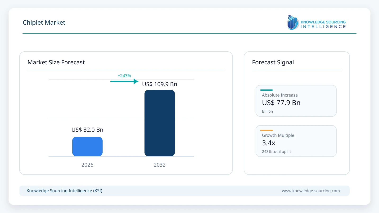
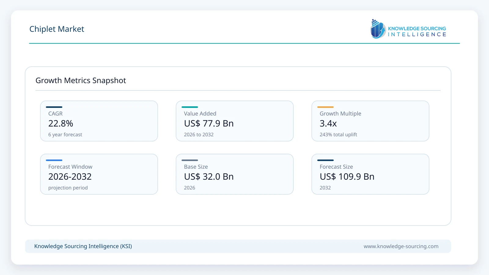
The Chiplet Market is estimated at USD 32.0 billion in 2026 and is projected to reach USD 109.9 billion by 2032, representing a CAGR of 22.8% over 2026-2032.
Highlights:
- 1Data-center CPUs and AI accelerators represent the largest chiplet revenue application in 2026.
- 23D and hybrid-stacked chiplet architectures are the fastest-growing integration form through 2032.
- 3UCIe 3.0 doubles standardized die-to-die bandwidth to support larger interoperable chiplet systems.
- 4Broadcom began shipping 2 nm 3.5D chiplet-based custom AI compute silicon during 2026.
- 5North America leads chiplet design and commercialization while Asia Pacific dominates manufacturing integration.
The economic case for chiplets begins with die size and yield. As monolithic processors become larger, the probability of a defect affecting the complete die increases and the cost of manufacturing every transistor on the newest process node becomes harder to justify. Partitioning a design into smaller dies can improve manufacturability and lets non-critical I/O, cache or analog functions remain on more mature nodes. AMD demonstrated this model at scale in server and client processors, and the same principle is now extending into AI accelerators, custom XPUs, networking silicon and heterogeneous compute systems.
The technology is also changing from proprietary multi-chip modules toward more modular design ecosystems. UCIe provides a standardized physical and protocol framework for die-to-die communication, while Arm Chiplet System Architecture adds system-level conventions intended to improve reuse and interoperability. Proprietary fabrics remain important because tightly optimized CPU, GPU and accelerator products can still justify custom links, but open chiplet standards lower the engineering barrier for companies that cannot build a complete monolithic system-on-chip from scratch.
Advanced packaging is an enabling layer rather than the same market. TSMC CoWoS and SoIC, Intel EMIB and Foveros, Broadcom 3.5D XDSiP, ASE FOCoS and other platforms create the physical integration needed to connect several dies with high bandwidth and low power. The chiplet market counted here recognizes the semiconductor and interface value of those modular dies, while excluding the separate assembly, interposer, substrate and manufacturing-equipment revenue. This distinction becomes increasingly important as package value rises alongside chiplet count.
Market Drivers
AI accelerators are exceeding the practical limits of monolithic scaling
AI training and inference processors require more compute, memory bandwidth and I/O than can be economically integrated within one reticle-limited die. AMD Instinct MI350 processors use eight accelerator complex dies and two I/O dies, while Broadcom is shipping 3.5D custom AI silicon that combines multiple stacked compute dies, I/O chiplets and HBM within one system-in-package. Partitioning the design allows logic blocks to scale independently and creates a direct revenue opportunity for specialized compute and I/O chiplets.
Node optimization improves cost and development flexibility
Not every function benefits equally from the newest process technology. Compute arrays may justify 2 nm or 3 nm fabrication, while I/O, analog and selected cache functions can remain on older nodes with better cost structures. Chiplets let designers combine those dies without forcing the complete device onto one expensive process. The approach also reduces the amount of new silicon that must be redesigned when a product family changes, allowing proven I/O or control chiplets to be reused across multiple compute generations.
Open die-to-die standards broaden the addressable supplier base
Standardized chiplet interfaces reduce the dependence on one vertically integrated supplier. UCIe 3.0 supports 48 GT/s and 64 GT/s links and adds management, sideband and power-control features needed for more complex multi-die systems. Arm Compute Subsystems and Chiplet System Architecture similarly provide reusable compute and system building blocks that can connect through UCIe or partner-specific physical layers. These developments create a path for merchant chiplet IP and specialized silicon suppliers to participate in systems that previously required one company to design every die.
Advanced packaging capacity is expanding around heterogeneous integration
Foundries and outsourced semiconductor assembly and test providers are adding capacity for larger multi-die packages, improving the manufacturing base available for chiplet products. Intel is expanding U.S. Foveros and EMIB capability, TSMC continues to scale CoWoS and SoIC, and ASE announced new AI packaging capacity and panel-level production development during 2026. More packaging capacity reduces one of the principal bottlenecks to broader chiplet commercialization and supports higher shipment volumes across AI, data-center and custom-compute products.
Restraints and Adoption Challenges
Chiplets shift complexity rather than eliminate it. Designers must manage die-to-die latency, power delivery, clocking, thermal gradients, test coverage, known-good-die yield and package warpage across several components. Interoperability remains limited because many commercial products still use proprietary interfaces even as UCIe adoption expands. Multi-vendor systems also require clear ownership of validation and failure analysis when a package combines dies from different suppliers. For lower-cost or lower-performance devices, a monolithic system-on-chip can remain economically superior because the added package, interface and test complexity of chiplets is not justified.
Chiplet Market Segment Analysis
By Application
Data-center CPUs and AI accelerators represent the largest chiplet revenue application in 2026 because they combine the highest device values with the strongest economic need to exceed monolithic die limits. AMD EPYC and Instinct, Intel data-center processors and GPUs, Broadcom custom XPUs and other hyperscale silicon programs increasingly partition compute and I/O functions across multiple dies. The amount of chiplet semiconductor content per package is substantially higher than in mainstream embedded or consumer applications.
Automotive, edge and specialized custom compute are expected to expand from a smaller base, but the fastest integration transition occurs within 3D and hybrid-stacked AI and high-performance computing systems. Face-to-face hybrid bonding and dense vertical links allow designers to place compute, cache, I/O or control dies much closer together than conventional 2.5D layouts. Broadcom is already shipping a 3.5D custom AI device, while Intel and TSMC are scaling hybrid-bonded 3D integration for future products.
Chiplet Category | Revenue Contribution | Growth Direction | Primary Application |
Compute chiplets | Largest category | Very strong | Server CPUs, AI accelerators and high-performance processors |
I/O and control chiplets | Large established category | Strong | Memory, PCIe, networking and platform I/O integration |
Accelerator and specialized-function chiplets | Growing high-value category | Very strong | AI, security, signal processing and workload-specific compute |
3D-stacked logic chiplets | Smaller 2026 base | Fastest | Dense AI/HPC integration with short die-to-die links |
Interface and die-to-die IP | Supporting ecosystem | Very strong | UCIe and proprietary interconnect implementation |
Photonic and mixed-domain chiplets | Emerging | Fast | Optical I/O and heterogeneous electrical-photonic systems |
Market and Technology Indicators
Indicator | Revenue Contribution | Market Impact |
AMD multi-die compute | AMD MI350 integrates eight accelerator complex dies and two I/O dies in one package. | Confirms large-scale commercial chiplet deployment in AI accelerators. |
Broadcom 3.5D production | Broadcom began shipping a 2 nm custom compute SoC using 3.5D face-to-face integration in February 2026. | Moves stacked chiplet architecture into production custom AI silicon. |
Intel advanced packaging | Intel is scaling EMIB, Foveros and Foveros Direct for multi-chip AI and data-center systems. | Expands foundry and IDM support for heterogeneous chiplet products. |
UCIe 3.0 ecosystem | UCIe 3.0 supports 48 GT/s and 64 GT/s with enhanced manageability. | Improves bandwidth and interoperability for open chiplet systems. |
Arm chiplet-ready subsystems | Arm Neoverse CSS supports chiplet and multi-die designs with UCIe or partner PHYs. | Lowers development barriers for custom cloud and AI silicon. |
Advanced packaging expansion | ASE is expanding AI packaging and panel-level capability for chiplet and HBM integration. | Increases manufacturing capacity available for complex multi-die systems. |
Regional Opportunity
North America
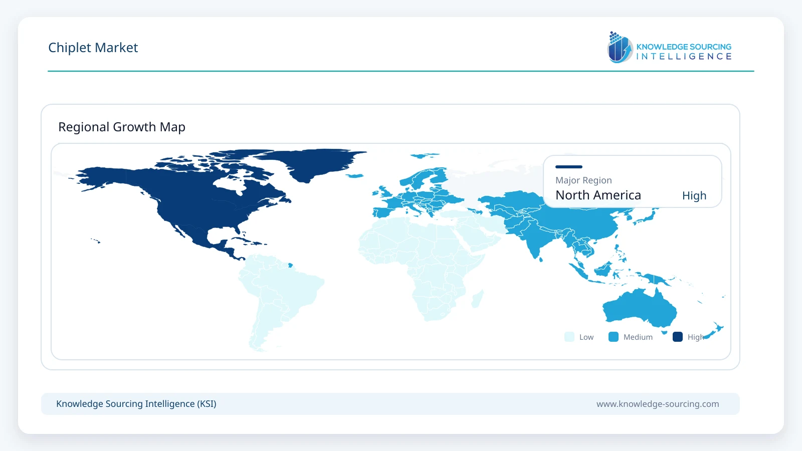
North America is the leading chiplet design and commercialization market because the United States contains many of the companies driving multi-die processor and accelerator architectures. AMD established chiplet CPUs at high volume and now uses heterogeneous chiplets across EPYC and Instinct products. Intel combines processor tiles with EMIB and Foveros and is offering advanced packaging to external foundry customers. NVIDIA, Broadcom and Marvell are increasing chiplet content in AI, networking and custom-compute systems, while Arm, Synopsys and Cadence provide system, interface and design IP used across multi-die projects.
AI infrastructure is the strongest incremental demand source. Broadcom began shipping its 3.5D custom XPU platform in 2026, and hyperscale customers are increasingly using custom accelerators that combine compute, I/O and memory interfaces across several dies. The value of chipletization is particularly high in these products because leading-edge compute can be separated from reusable I/O, SerDes and control functions, reducing the amount of advanced-node silicon required for each design revision.
The region also benefits from expanding domestic packaging capability. Intel is investing in U.S. advanced packaging, while Amkor and other suppliers are developing additional North American capacity. This does not displace Asia Pacific as the principal manufacturing base, but it improves supply-chain diversity for high-value chiplet products and creates more options for defense, sovereign and hyperscale customers that place greater weight on geographically resilient production.
Asia Pacific remains the dominant manufacturing and packaging region through TSMC, Samsung Electronics, ASE, Amkor operations, memory suppliers and a dense electronics supply chain. Europe participates through automotive, industrial, semiconductor IP and research ecosystems. Other regions remain smaller in direct chiplet production but increasingly consume chiplet-based systems through cloud, AI and networking infrastructure.
Competitive Landscape
Competition spans processor vendors, custom-silicon suppliers, foundries, packaging companies and semiconductor IP providers. AMD remains one of the most mature commercial chiplet users across CPUs and accelerators. Intel combines internal product deployment with external foundry packaging, while NVIDIA increasingly relies on multi-die and heterogeneous integration in large AI systems. Broadcom and Marvell are expanding custom AI and networking silicon using chiplet and advanced system-in-package architectures for hyperscale customers.
Foundry and packaging capability is strategically important because chiplet products depend on dense die-to-die interconnect and large package integration. TSMC provides CoWoS and SoIC, Intel offers EMIB and Foveros, Samsung Electronics develops advanced multi-die integration, and ASE and Amkor provide outsourced assembly and packaging platforms. Their role is enabling rather than identical to the chiplet semiconductor revenue counted in this study.
IP and design-tool suppliers are becoming more important as the ecosystem opens. Arm Chiplet System Architecture and Compute Subsystems give designers reusable compute building blocks; Synopsys and Cadence provide UCIe PHY, controller, verification and multi-die design tools. Competitive advantage increasingly depends on reusable silicon IP, process-node flexibility, die-to-die bandwidth, packaging qualification and the ability to validate complex heterogeneous systems before tape-out.
Major companies and ecosystem participants covered: AMD, Intel, NVIDIA, Broadcom, Marvell Technology, TSMC, Samsung Electronics, ASE Technology Holding, Amkor Technology, Arm, Synopsys, Cadence Design Systems, MediaTek, Qualcomm and Tenstorrent.
Recent Developments
August 2026: Intel outlined next-generation agentic-AI architectures using Foveros Direct 3D packaging and early UCIe adoption for open chiplet interconnects.
August 2026: The UCIe Consortium highlighted growing commercial interest in UCIe 3.0 as an open foundation for scalable interoperable chiplet architectures.
July 2026: Intel Foundry detailed expanded use of Foveros, EMIB and EMIB-T to scale multi-chip AI semiconductors beyond conventional reticle limits.
May 2026: ASE announced an automated 310 mm by 310 mm panel-level packaging production line aligned with chiplet, ASIC and HBM integration for AI workloads.
February 2026: Broadcom began shipping a 2 nm custom AI compute SoC using its 3.5D XDSiP face-to-face chiplet integration platform.
2026: AMD continued commercial rollout of MI350 Series accelerators using eight compute chiplets and two I/O dies connected through on-package Infinity Fabric.
2026: Arm expanded chiplet-ready Neoverse Compute Subsystems supporting UCIe and partner-specific die-to-die physical interfaces.
2026: TSMC continued volume scaling of SoIC and CoWoS platforms for heterogeneous chiplet integration across AI and high-performance computing products.
Chiplet Market Scope:
| Report Metric | Details |
|---|---|
| Total Market Size in 2026 | USD 32.0 billion |
| Total Market Size in 2032 | USD 109.9 billion |
| Forecast Unit | USD Billion |
| Growth Rate | 22.8% |
| Study Period | 2021 to 2032 |
| Historical Data | 2021 to 2024 |
| Base Year | 2025 |
| Forecast Period | 2026 – 2032 |
| Segmentation | Chiplet Function, Integration Architecture, Interconnect Approach, Application, Provider Type, Geography |
| Companies |
|
Market Segmentation
By Chiplet Function
Compute Chiplets
I/O and Control Chiplets
Accelerator and Specialized-Function Chiplets
Interface and Die-to-Die Chiplets
Photonic and Mixed-Domain Chiplets
By Integration Architecture
2D / Multi-Chip Module
2.5D Interposer and Bridge Integration
3D Stacked Chiplets
Hybrid 2.5D / 3D and 3.5D Architectures
By Interconnect Approach
Proprietary Die-to-Die Interconnects
UCIe-Based Interconnects
AMBA CHI C2C and Other Open Interfaces
Hybrid and Application-Specific Interconnects
By Application
Data Center CPUs
AI Accelerators and Custom XPUs
Client Computing
Networking and Communications
Automotive
Industrial, Edge and Other Applications
By Provider Type
Integrated Device Manufacturers
Fabless Semiconductor Companies
Custom Silicon and ASIC Providers
Foundry and Advanced Packaging Ecosystem
Semiconductor IP and Design Tool Providers
By Geography
North America
United States
Canada
Europe
Asia Pacific
Middle East and Rest of World
Table of Contents
1. EXECUTIVE SUMMARY
1.1. Market Opportunity and Key Findings
1.2. Chiplet Adoption Outlook
1.3. Principal Revenue Pools
2. MARKET OVERVIEW
2.1. Evolution from Monolithic SoCs to Chiplets
2.2. Chiplet Economics and Yield Advantages
2.3. Die-to-Die Interconnect and System Integration
2.4. Advanced Packaging and Heterogeneous Integration
2.5. Open versus Proprietary Chiplet Ecosystems
3. MARKET SIZE AND FORECAST, 2026-2032
3.1. Global Market Revenue
3.2. Annual Growth Analysis
3.3. Chiplet Content per Semiconductor Package
3.4. Adoption by Compute Platform
4. MARKET BY CHIPLET FUNCTION
4.1. Compute Chiplets
4.2. I/O and Control Chiplets
4.3. Accelerator and Specialized-Function Chiplets
4.4. Interface and Die-to-Die Chiplets
4.5. Photonic and Mixed-Domain Chiplets
5. MARKET BY INTEGRATION ARCHITECTURE
5.1. 2D / Multi-Chip Module
5.2. 2.5D Interposer and Bridge Integration
5.3. 3D Stacked Chiplets
5.4. Hybrid 2.5D / 3D and 3.5D Architectures
6. MARKET BY INTERCONNECT APPROACH
6.1. Proprietary Die-to-Die Interconnects
6.2. UCIe-Based Interconnects
6.3. AMBA CHI C2C and Other Open Interfaces
6.4. Hybrid and Application-Specific Interconnects
7. MARKET BY APPLICATION
7.1. Data Center CPUs
7.2. AI Accelerators and Custom XPUs
7.3. Client Computing
7.4. Networking and Communications
7.5. Automotive
7.6. Industrial, Edge and Other Applications
8. MARKET BY PROVIDER TYPE
8.1. Integrated Device Manufacturers
8.2. Fabless Semiconductor Companies
8.3. Custom Silicon and ASIC Providers
8.4. Foundry and Advanced Packaging Ecosystem
8.5. Semiconductor IP and Design Tool Providers
9. REGIONAL MARKET
9.1. North America
9.1.1. United States
9.1.2. Canada
9.2. Europe
9.3. Asia Pacific
9.4. Middle East and Rest of World
10. MARKET DYNAMICS
10.1. Drivers
10.1.1. AI Accelerator Scaling beyond Monolithic Die Limits
10.1.2. Process-Node Optimization and Silicon Reuse
10.1.3. Open Die-to-Die Standards
10.1.4. Advanced Packaging Capacity Expansion
10.2. Restraints
10.2.1. Package and Thermal Complexity
10.2.2. Interoperability and Multi-Vendor Qualification
10.2.3. Known-Good-Die Test and Yield Management
10.2.4. Monolithic Economics in Lower-Cost Applications
11. COMPETITIVE LANDSCAPE
11.1. Market Structure and Competitive Intensity
11.2. Processor and Accelerator Chiplet Strategies
11.3. Custom Silicon and Merchant Chiplet Positioning
11.4. Foundry, Packaging and Manufacturing Ecosystem
11.5. IP, Design Tool and Interoperability Partnerships
12. COMPANY PROFILES
12.1. AMD
12.2. Intel
12.3. NVIDIA
12.4. Broadcom
12.5. Marvell Technology
12.6. TSMC
12.7. Samsung Electronics
12.8. ASE Technology Holding
12.9. Amkor Technology
12.10. Arm
12.11. Synopsys
12.12. Cadence Design Systems
12.13. MediaTek
12.14. Qualcomm
12.15. Tenstorrent
13. RECENT DEVELOPMENTS
14. APPENDIX
Navigate
Trusted by the world's leading organizations











