
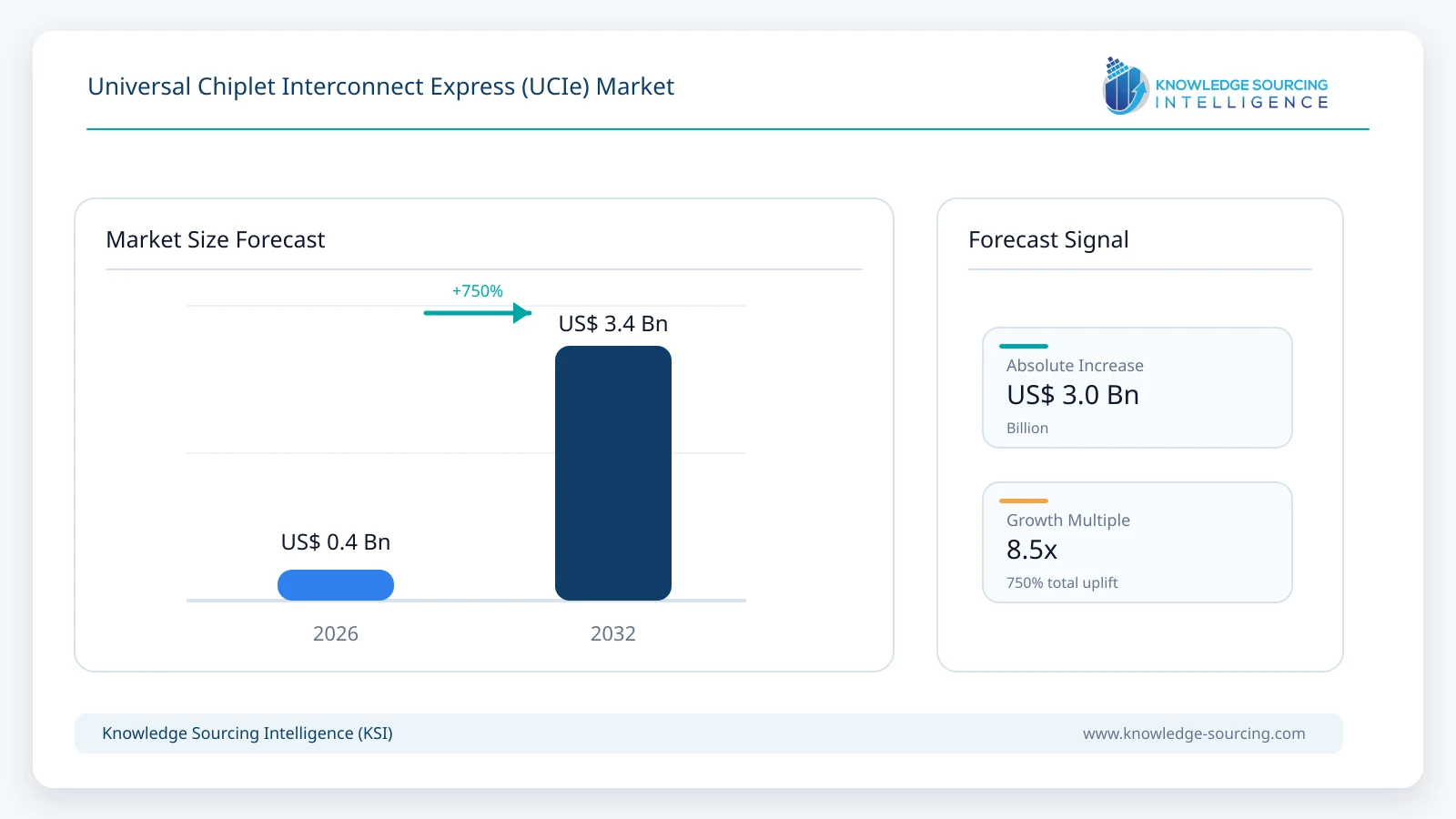
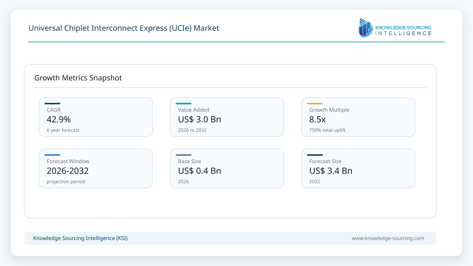
The Universal Chiplet Interconnect Express (UCIe) Market is estimated at USD 0.40 billion in 2026 and is projected to reach USD 3.40 billion by 2032, representing a CAGR of 42.9% during the forecast period.
Highlights:
- 1UCIe 3.0 raises supported data rates to 48 GT/s and 64 GT/s for next-generation chiplet systems.
- 2Cross-vendor interoperability moved from specification goals to live silicon demonstrations during 2026.
- 3AI and high-performance computing remain the strongest near-term drivers for production UCIe adoption.
- 4Verification, compliance and package co-design become more valuable as multi-vendor chiplet programs expand.
- 5Automotive, optical and configurable-compute applications broaden the addressable market beyond data centers.
Market Overview
Chiplet architectures divide functions that would traditionally reside on one large monolithic system-on-chip into smaller dies that can be manufactured separately and integrated within a common package. This approach can improve yield, allow process-node specialization and enable reuse of proven intellectual property, but it also creates a connectivity problem. Proprietary die-to-die interfaces work well inside vertically integrated product families but make it difficult to combine dies from different suppliers. UCIe addresses this problem by defining a common die-to-die interface that can transport established protocols such as PCI Express and Compute Express Link while also supporting streaming and vendor-defined traffic.
The commercial opportunity sits around implementation rather than ownership of the standard. Semiconductor designers require physical-layer IP, controllers, adapter logic, verification environments, package models, signal-integrity analysis, compliance testing and silicon-debug capabilities. Each new process node and package architecture creates additional qualification requirements because UCIe performance depends on both die circuitry and the package channel. Standard-package implementations target lower-cost organic packages, while advanced-package implementations use fine-pitch interconnects to reach substantially higher bandwidth density. UCIe 2.0 also introduced support for three-dimensional packaging, including hybrid-bonded structures, while UCIe 3.0 doubled the maximum data rate from 32 GT/s to 64 GT/s.
Adoption is likely to progress unevenly. Large cloud, processor and accelerator vendors can deploy internal chiplet interfaces without waiting for an open marketplace, but UCIe becomes more valuable when a design incorporates third-party chiplets or when a reusable die must serve several customers. The strongest early commercial opportunities therefore exist in interface IP, verification and integration tools that reduce implementation risk before a broad merchant chiplet marketplace is fully established.
Market Drivers
AI and HPC architectures require scalable die-to-die bandwidth
Artificial intelligence and high-performance computing devices are increasingly built from multiple compute, memory and input/output dies because leading-edge monolithic chips face reticle-size, yield and cost constraints. As packages integrate more dies, the amount of data transferred inside the package rises sharply and interconnect power becomes a system-level limitation. UCIe 3.0 addresses this requirement with 48 GT/s and 64 GT/s operation while maintaining backward compatibility. Cadence and Synopsys are already developing and taping out 64G-class UCIe IP, indicating that the design ecosystem is preparing for production programs that require substantially higher bandwidth density than first-generation implementations.
Open interfaces reduce the cost of reusable and multi-vendor chiplet platforms
Chiplets create the greatest economic advantage when proven dies can be reused across several products rather than redesigned for each system. A standardized interface allows compute, memory, radio-frequency, security or accelerator chiplets to be developed on the process node best suited to each function and connected at package level. AMD is extending this model to selected Versal RF Series devices, where UCIe can connect co-packaged chiplets for radio-frequency conversion, artificial intelligence, central processing units, graphics processing units, security and application-specific functions. Wider adoption can therefore shift UCIe from a connectivity feature into a platform-enablement requirement.
Interoperability testing is becoming a commercial requirement
A written standard does not guarantee that independently designed chiplets will operate together. PHY behavior, training, sideband signaling, package channels, error handling and protocol mappings must be validated across vendors. The Intel and Cadence live UCIe-S demonstration at Chiplet Summit 2026 was important because it connected independently designed chiplets and validated cross-vendor operation in silicon. As more suppliers enter the ecosystem, design teams will require verification IP, compliance software, test equipment, protocol analysis and structured interoperability programs, expanding revenue beyond the interface IP itself.
3D packaging and new application classes expand the implementation envelope
UCIe is extending beyond conventional side-by-side chiplet placement. UCIe 2.0 introduced support for 3D packaging and fine-pitch hybrid-bonding environments, while UCIe 3.0 added higher data rates, longer sideband reach and additional manageability features. The consortium is also developing application-specific guidance for automotive systems, where reliability, health monitoring and long product lifecycles are important. These extensions broaden the market for interface IP, verification and test solutions across vertical stacking, automotive compute, optical chiplets and other heterogeneous systems.
Restraints and Adoption Challenges
The principal constraint is that ecosystem readiness develops more slowly than specification capability. A multi-vendor chiplet requires aligned electrical characteristics, package design rules, thermal behavior, security assumptions, test coverage, firmware initialization and supply-chain qualification. Designers may therefore continue using proprietary die-to-die interfaces when they control all dies in a package and value optimization over interoperability. UCIe implementation can also add verification and compliance work before reusable chiplets generate economic benefits. Advanced-package versions depend on fine-pitch assembly and high-yield packaging, while three-dimensional implementations introduce additional thermal and test complexity. Production adoption will therefore be concentrated first in applications where chiplet reuse, external sourcing or platform flexibility justify the integration cost.
Technology and Application Analysis
By Enablement Layer
Physical-layer and controller IP form the foundation of the commercial UCIe ecosystem because every UCIe-enabled die requires compliant transmit, receive, training and protocol-interface functions. Cadence, Synopsys and Qualcomm through the former Alphawave Semi organization are among the suppliers developing die-to-die connectivity IP for advanced process nodes and package types. Verification IP is closely linked because designers must exercise protocol behavior, link states, lane repair, sideband communication and error conditions before tape-out. Siemens provides UCIe verification IP supporting the die-to-die adapter and logical PHY layers together with PCI Express and Compute Express Link operation over UCIe.
Compliance, test and package-analysis tools form a separate but increasingly important layer. UCIe performance depends on the combined die and package channel, requiring electrical models, voltage-transfer-function analysis, interoperability testing and silicon characterization. Keysight has incorporated UCIe 3.0 support into its chiplet design environment, including quarter-rate clock measurement and channel modeling. As production designs move toward 64 GT/s and 3D integration, test complexity increases and creates recurring demand for measurement hardware, software and engineering support.
By Application
Artificial intelligence accelerators and high-performance computing processors are the primary near-term applications because they already use multi-die architectures and require extreme bandwidth density. Data-center networking and custom cloud silicon follow for similar reasons, especially where compute, memory, optical input/output or network functions can be developed as reusable chiplets. Client and edge processors are beginning to adopt chiplet approaches at lower cost points, while automotive platforms represent a longer-cycle opportunity that benefits from modular compute and reuse across vehicle programs. Optical and memory chiplets create additional opportunities as system architects move high-bandwidth data movement closer to compute dies.
Technology and Commercialization Indicators
Indicator | Current evidence | Market implication |
UCIe 3.0 performance | Supports 48 GT/s and 64 GT/s, doubling the maximum UCIe 2.0 data rate. | Raises requirements for PHY IP, package analysis, verification and test. |
Cross-vendor interoperability | Intel and Cadence demonstrated live UCIe-S interoperability at Chiplet Summit 2026. | Reduces perceived risk of independently designed chiplets operating together. |
64G IP readiness | Cadence and Synopsys have announced 64G-class UCIe IP development and tape-outs. | Positions ecosystem vendors for next-generation AI and HPC programs. |
Production roadmap | AMD plans native UCIe connectivity in selected Versal RF Series devices, with production chiplets expected in Q4 2027. | Moves UCIe from test platforms toward commercial configurable-compute products. |
3D and hybrid bonding | UCIe 2.0 supports 3D packaging across fine-pitch hybrid-bonding geometries. | Extends the standard into vertically integrated multi-die systems. |
Automotive expansion | UCIe Consortium automotive activity addresses reliability and scalable modular compute. | Broadens long-term adoption beyond data-center and HPC systems. |
Regional Opportunity
North America
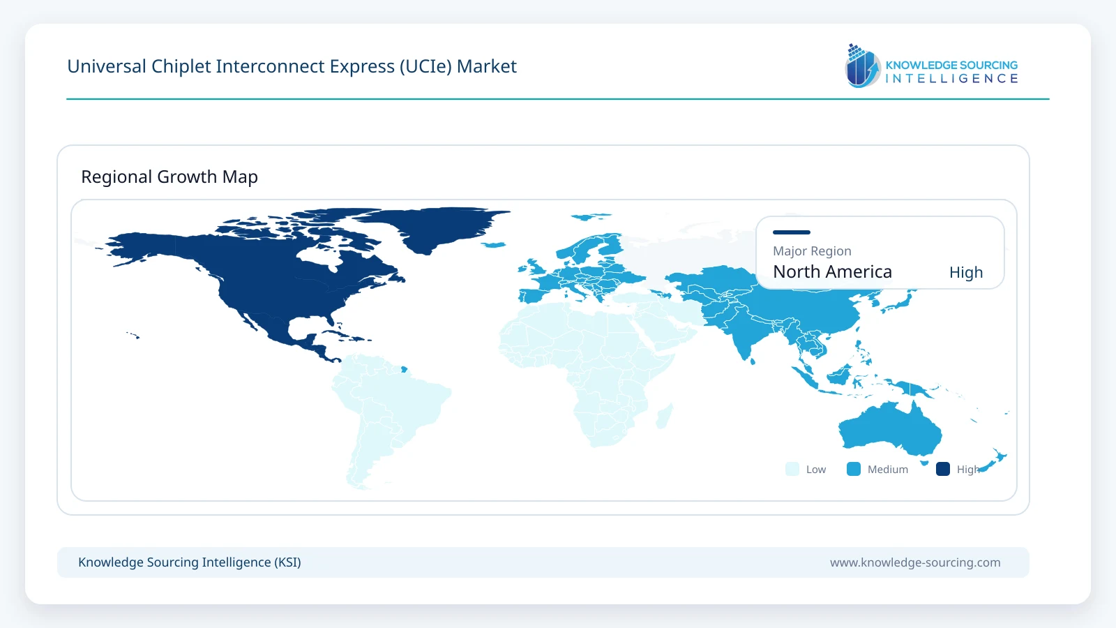
North America is the strongest early commercial region for UCIe enablement because the United States contains a dense concentration of processor vendors, cloud companies, design-automation suppliers, interface-IP developers and test-equipment companies. Intel, AMD, NVIDIA, Qualcomm, Google, Microsoft and Meta are represented in the UCIe promoter ecosystem, while Cadence, Synopsys, Siemens EDA and Keysight provide core implementation and validation tools. This combination creates demand across the full design cycle, from architecture and IP selection to package co-design, verification, characterization and interoperability testing.
The region is also important because several early production programs are being driven by U.S.-based semiconductor companies. Intel has demonstrated early UCIe adoption in processor roadmaps and participated in live cross-vendor interoperability testing. AMD announced native UCIe connectivity for selected Versal adaptive system-on-chips, creating a platform intended to attach specialized third-party or internally developed chiplets. Qualcomm gained additional high-speed connectivity and chiplet capabilities through its acquisition of Alphawave Semi, strengthening another commercial UCIe-capable supplier within the North American ecosystem.
Cloud and artificial intelligence infrastructure add a second demand layer. Large hyperscalers increasingly design custom accelerators and infrastructure silicon, making reusable chiplets and open die-to-die connectivity attractive where internal silicon programs need to combine compute, memory, input/output or security functions. UCIe does not require these companies to buy merchant chiplets immediately; adoption can begin with internal reusable dies and later expand to multi-vendor sourcing as interoperability matures. This phased path supports demand for commercial IP and design tools before a fully open chiplet marketplace develops.
Asia Pacific remains essential through semiconductor fabrication, advanced packaging and system manufacturing. TSMC, Samsung and ASE are promoter members and can support UCIe-enabled designs through foundry and packaging ecosystems. Taiwan and South Korea are particularly important for advanced packaging, while Japan and Southeast Asia contribute materials, test and assembly capabilities. Europe participates through automotive semiconductor demand, processor architecture, design services and verification technologies, with automotive likely to become more meaningful as reliability-focused UCIe implementations mature.
Competitive Landscape
The competitive landscape combines interface-IP suppliers, electronic design automation vendors, semiconductor companies, foundries, advanced packaging providers and test-equipment companies. Cadence and Synopsys compete most directly in complete UCIe IP subsystems spanning controller, PHY and verification. Siemens participates strongly in verification IP and multi-die design workflows. Qualcomm incorporates high-speed wired connectivity and chiplet technology acquired with Alphawave Semi, while Intel has contributed both technology development and interoperability demonstrations.
Semiconductor and manufacturing companies shape the market even when they do not sell UCIe IP directly. AMD is moving UCIe into configurable compute platforms, while Arm, NVIDIA and other architecture or processor companies influence interface requirements for reusable chiplets. TSMC, Samsung and ASE provide the process, package and qualification environments in which UCIe IP must operate. Keysight and other measurement companies participate through channel analysis, electrical validation and compliance tools. Specialized companies such as Eliyan, proteanTecs and VeriSilicon add die-to-die connectivity, monitoring, design and integration capabilities around the broader chiplet ecosystem.
Competitive differentiation depends on silicon proof, process portability, package support, interoperability and complete design enablement rather than peak data rate alone. Customers need working controller and PHY IP, verification environments, known-good package models, debug visibility and reliable bring-up across process-voltage-temperature conditions. Suppliers able to demonstrate multi-vendor interoperability and support both standard and advanced packaging are better positioned as UCIe moves into production programs.
Ecosystem Positioning
Participant group | Role in UCIe ecosystem | Current direction |
Cadence | UCIe controller/PHY IP, verification, 3D-IC and package analysis | 64G IP, cross-vendor interoperability and broader chiplet partner ecosystem. |
Synopsys | Controller, PHY, verification IP and multi-die design enablement | 64G tape-outs and silicon-proven operation across advanced nodes. |
Siemens EDA | Verification IP and multi-die verification workflows | Protocol, adapter and logical-PHY verification for UCIe-based systems. |
Qualcomm / former Alphawave Semi | High-speed connectivity IP, custom silicon and chiplet technology | Integration into Qualcomm data-center and heterogeneous-compute strategy. |
Intel and AMD | Processor and adaptive-compute adopters | Interoperability demonstrations and production UCIe platform roadmaps. |
TSMC, Samsung and ASE | Foundry and advanced-packaging ecosystem | Process/package qualification and manufacturing support for UCIe designs. |
Keysight and test ecosystem | Electrical design, channel analysis and compliance validation | UCIe 3.0 modeling and high-speed chiplet measurement workflows. |
Recent Developments
August 2026: AMD announced native UCIe 1.1 connectivity for selected Versal RF Series adaptive SoCs, with production chiplets expected in the fourth quarter of 2027.
August 2026: Synopsys detailed its 64G UCIe IP roadmap and tape-outs across advanced 2 nm and 3 nm process technologies for multi-die AI and HPC systems.
July 2026: Samsung Foundry and Cadence expanded their AI design collaboration, including UCIe 64G interface IP within the advanced connectivity portfolio for next-generation 2 nm platforms.
July 2026: The UCIe Consortium expanded automotive ecosystem activity around modular compute, reliability, interoperability and long-lifecycle semiconductor requirements.
March 2026: Intel and Cadence demonstrated the industry's first live UCIe-S cross-vendor interoperability using independently designed 16G UCIe chiplets.
August 2025: The UCIe Consortium released UCIe 3.0 with 48 GT/s and 64 GT/s support, extended sideband reach and enhanced manageability and power features.
Universal Chiplet Interconnect Express (UCIe) Market Scope:
| Report Metric | Details |
|---|---|
| Total Market Size in 2026 | USD 0.40 billion |
| Total Market Size in 2032 | USD 3.40 billion |
| Forecast Unit | USD Billion |
| Growth Rate | 42.9% |
| Study Period | 2021 to 2032 |
| Historical Data | 2021 to 2024 |
| Base Year | 2025 |
| Forecast Period | 2026 – 2032 |
| Segmentation | Enablement Layer, UCIe Generation, Package Type, Application, Customer Type, Geography |
| Companies |
|
Market Segmentation
By Enablement Layer
UCIe Controller and Protocol IP
UCIe PHY IP
Verification IP
Design, Package and Signal-Integrity Software
Compliance and Interoperability Test Systems
Integration, Bring-Up and Engineering Services
By UCIe Generation
UCIe 1.x Implementations
UCIe 2.0 and 3D Packaging
UCIe 3.0 48G and 64G Implementations
Future Specification Evolution
By Package Type
Standard Package UCIe
Advanced Package UCIe
2.5D Interposer and Bridge Packages
3D and Hybrid-Bonded Multi-Die Systems
By Application
AI Accelerators and GPUs
High-Performance Computing and Server CPUs
Data-Center Networking and Custom Cloud Silicon
Client and Edge Computing
Automotive Compute
Optical, Memory and Specialized Chiplets
By Customer Type
Fabless Semiconductor Companies
Integrated Device Manufacturers
Cloud and Hyperscale Silicon Developers
Foundries and Advanced Packaging Providers
Automotive and Industrial Semiconductor Companies
IP, EDA and Design-Service Providers
By Geography
North America
United States
Canada
Asia Pacific
Taiwan
South Korea
Japan
China and Southeast Asia
Europe
Rest of World
Table of Contents
1. EXECUTIVE SUMMARY
1.1. Market Opportunity and Key Findings
1.2. UCIe Commercialization Outlook
1.3. Open Chiplet Ecosystem Development
2. MARKET OVERVIEW
2.1. UCIe Architecture and Role in Multi-Die Systems
2.2. Die-to-Die Physical Layer and Adapter Architecture
2.3. PCI Express, Compute Express Link and Streaming Protocol Support
2.4. Standard Package and Advanced Package Implementations
2.5. UCIe 3D and Hybrid-Bonded Architectures
2.6. Interoperability, Manageability and Debug
3. MARKET SIZE AND FORECAST, 2026-2032
3.1. Global Market Revenue
3.2. Commercialization and Production Ramp
3.3. UCIe-Enabled Design Program Outlook
4. MARKET BY ENABLEMENT LAYER
4.1. UCIe Controller and Protocol IP
4.2. UCIe PHY IP
4.3. Verification IP
4.4. Design, Package and Signal-Integrity Software
4.5. Compliance and Interoperability Test Systems
4.6. Integration, Bring-Up and Engineering Services
5. MARKET BY UCIE GENERATION
5.1. UCIe 1.x Implementations
5.2. UCIe 2.0 and 3D Packaging
5.3. UCIe 3.0 48G and 64G Implementations
5.4. Future Specification Evolution
6. MARKET BY PACKAGE TYPE
6.1. Standard Package UCIe
6.2. Advanced Package UCIe
6.3. 2.5D Interposer and Bridge Packages
6.4. 3D and Hybrid-Bonded Multi-Die Systems
7. MARKET BY APPLICATION
7.1. AI Accelerators and GPUs
7.2. High-Performance Computing and Server CPUs
7.3. Data-Center Networking and Custom Cloud Silicon
7.4. Client and Edge Computing
7.5. Automotive Compute
7.6. Optical, Memory and Specialized Chiplets
8. MARKET BY CUSTOMER TYPE
8.1. Fabless Semiconductor Companies
8.2. Integrated Device Manufacturers
8.3. Cloud and Hyperscale Silicon Developers
8.4. Foundries and Advanced Packaging Providers
8.5. Automotive and Industrial Semiconductor Companies
8.6. IP, EDA and Design-Service Providers
9. REGIONAL MARKET
9.1. North America
9.1.1. United States
9.1.2. Canada
9.2. Asia Pacific
9.2.1. Taiwan
9.2.2. South Korea
9.2.3. Japan
9.2.4. China and Southeast Asia
9.3. Europe
9.4. Rest of World
10. MARKET DYNAMICS
10.1. Drivers
10.1.1. AI and HPC Die-to-Die Bandwidth Requirements
10.1.2. Reusable and Multi-Vendor Chiplet Platforms
10.1.3. Interoperability and Compliance Requirements
10.1.4. 3D Packaging and New Application Classes
10.2. Restraints
10.2.1. Multi-Vendor Integration and Qualification Complexity
10.2.2. Competition from Proprietary Die-to-Die Interfaces
10.2.3. Advanced Packaging Yield and Cost
10.2.4. Production Adoption Lag versus Specification Development
11. COMPETITIVE LANDSCAPE
11.1. Market Structure and Commercial Readiness
11.2. Controller and PHY IP Competition
11.3. Verification and Multi-Die Design Platforms
11.4. Compliance, Test and Interoperability Ecosystem
11.5. Foundry and Advanced Packaging Partnerships
12. COMPANY PROFILES
12.1. Cadence Design Systems
12.2. Synopsys
12.3. Siemens EDA
12.4. Intel
12.5. AMD
12.6. Qualcomm
12.7. Arm
12.8. NVIDIA
12.9. Taiwan Semiconductor Manufacturing Company
12.10. Samsung Electronics
12.11. ASE Technology Holding
12.12. Keysight Technologies
12.13. Eliyan
12.14. proteanTecs
12.15. VeriSilicon
13. RECENT DEVELOPMENTS
14. APPENDIX
Navigate
Trusted by the world's leading organizations











