
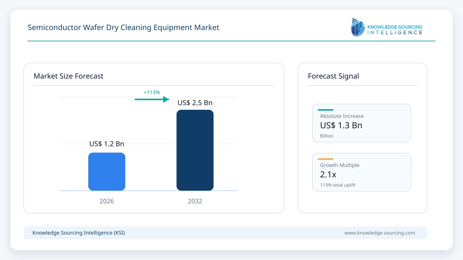
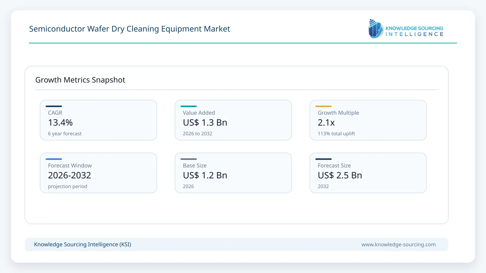
The Semiconductor Wafer Dry Cleaning Equipment Market is estimated at USD 1.20 billion in 2026 and is projected to reach USD 2.55 billion by 2032, representing a CAGR of 13.4% during 2026-2032.
Highlights:
- 1Dry cleaning gains relevance where wet-process capillary forces can damage fragile high-aspect-ratio features.
- 2Plasma-enhanced and radical-based tools increasingly target selective oxide, nitride, silicon and residue removal.
- 3Hybrid bonding expands demand for low-damage pre-bond surface cleaning and activation.
- 4Cryogenic carbon-dioxide cleaning provides a chemical-free route for particles and thin organic contamination.
- 5Asia Pacific remains the largest opportunity due to its concentration of advanced logic, memory and packaging capacity.
Dry wafer cleaning covers several different process mechanisms. Plasma-enhanced systems use ions and radicals to remove surface contamination or thin unwanted films. Downstream and remote-plasma systems generate reactive species away from the wafer, reducing direct ion bombardment and making them attractive for low-damage cleaning. Radical-based selective removal can target oxide, nitride, silicon or other materials with high selectivity, which is increasingly useful in three-dimensional device structures where a wet chemistry may attack multiple exposed layers.
Gas-phase and cryogenic approaches solve different problems. Cryogenic carbon-dioxide systems direct controlled CO2 snow or particles across the wafer to remove particulates and organic residues without water, solvents or a subsequent drying step. Gas-phase selective cleans can remove native oxide or residue while the wafer remains under vacuum, helping reduce queue-time oxidation and contamination between process modules. These processes are often integrated close to deposition, bonding or contact-formation steps so the cleaned surface is not re-exposed before the next operation.
Hybrid bonding and three-dimensional integration are raising the value of surface preparation. Copper-to-copper and oxide-to-oxide bonding require extremely clean, flat and chemically controlled surfaces. Plasma treatment can remove organic contamination and activate dielectric surfaces while limiting particle generation. As hybrid bonding moves from image sensors into high-bandwidth memory, chiplets and logic-memory integration, dry cleaning is increasingly part of the bonding flow rather than only a front-end contact-clean step.
Market Drivers
High-aspect-ratio structures reduce the effectiveness of wet-only cleaning
Three-dimensional NAND, advanced DRAM capacitors and gate-all-around logic introduce narrow openings, deep channels and fragile structures that are difficult to clean uniformly using liquid chemistry. Liquids can experience transport limitations in deep features, while drying can create capillary forces that bend or collapse patterns. Applied Materials highlights fully dry selective removal as a way to preserve structural integrity in fragile high-aspect-ratio features, supporting greater use of gas- and radical-based cleaning steps.
Selective surface preparation becomes more important at advanced nodes
Advanced logic and memory increasingly require removal of only a few nanometers of oxide, damaged silicon, polymer or residue while leaving adjacent materials intact. PSK's INTEGER platforms emphasize controllable selectivity for oxide, nitride and poly-silicon removal, while radical-based dry clean systems can be tuned to specific materials. This creates value for equipment that combines high selectivity with low plasma damage and tight wafer-to-wafer repeatability.
Hybrid bonding creates a new pre-bond cleaning opportunity
Hybrid bonding requires low particle counts, controlled native oxide, low organic contamination and activated dielectric surfaces immediately before bonding. Plasma-based cleaning and activation can improve surface energy without introducing a liquid drying step. ULVAC presented surface-wave-excited downstream plasma for hybrid-bonding cleaning and activation at the 2026 IEEE Hybrid Bonding Symposium, illustrating how dry surface preparation is moving into advanced packaging and 3D integration.
Environmental and process-integration advantages support specialty dry cleans
Dry cleaning can reduce water use, solvent handling and hazardous liquid waste for selected process steps. Bruker's cryogenic CO2 system removes particles and thin organic residues without wet chemistry and is installed in high-volume applications. Vacuum-integrated dry cleans can also shorten queue time between cleaning and deposition or bonding, reducing reoxidation and airborne contamination. These benefits are most valuable in high-cost process modules where small defect reductions can materially improve yield.
Restraints and Adoption Challenges
Dry cleaning does not replace wet cleaning across the fab. Many contaminants are still removed more efficiently using liquid chemistries, and dry processes can introduce their own challenges including plasma damage, chamber seasoning, gas handling, residue redeposition and limited effectiveness against certain ionic or metallic contaminants. Equipment must also achieve high throughput to compete with mature wet platforms. Cryogenic systems require precise particle delivery and exhaust management, while selective gas-phase processes need tight chemistry control. Integration into existing fabs can be difficult when the dry clean must sit directly beside deposition, etch or bonding modules.
Segment Analysis
By Cleaning Technology
Plasma-enhanced and remote-plasma dry cleaners represent the largest commercial category because they can be used for native-oxide removal, high-aspect-ratio contact cleaning, damaged-silicon removal, organic residue removal and pre-bond surface preparation. Radical-based selective cleaning is becoming more important in advanced logic and memory because it allows targeted removal without the pattern-collapse risk associated with a subsequent liquid dry step. Cryogenic CO2 cleaning occupies a smaller but differentiated niche where particle removal and surface protection are prioritized.
The fastest technology development is occurring in integrated selective dry clean and hybrid-bonding surface preparation. These applications place more emphasis on atomic-scale selectivity, low ion energy, surface chemistry and in-vacuum transfer than on bulk contamination removal. Edge-cleaning systems are also gaining attention because film and particle accumulation at the wafer bevel can create defects during advanced deposition and bonding flows.
Technology | Primary Cleaning Function | Typical Applications | Commercial Direction |
Remote/downstream plasma | Low-damage radical cleaning and activation | Pre-bond clean, organic removal, oxide conditioning | Expanding with hybrid bonding and advanced packaging |
Plasma-enhanced selective clean | Controlled removal of oxide, nitride, silicon and residues | HAR contacts, DRAM, GAA logic | Core advanced-node dry-clean category |
Radical-based gas clean | Highly selective dry material removal | 3D NAND, DRAM, selective surface prep | Growing as structures become more three-dimensional |
Cryogenic CO2 clean | Particle and thin organic residue removal | MEMS, compound semiconductors, wafer surfaces | Specialty production niche with no wet chemistry |
Gas-phase native-oxide clean | Native oxide and interface preparation | Contacts, deposition preclean, silicide formation | Important where queue-time oxidation must be minimized |
Dry edge / bevel clean | Film and particle removal at wafer perimeter | Deposition, packaging and yield improvement | Increasing with edge-exclusion and bonding requirements |
Market and Technology Indicators
Indicator | Current Evidence | Market Impact |
Next-generation dry cleaning | PSK states that it is developing next-generation dry-cleaning solutions and has applied dry cleaning to 10 nm-class DRAM production. | Confirms dry clean is established in advanced memory and remains an active R&D area. |
High-aspect-ratio clean | PSK INTEGER tools support plasma-enhanced removal of oxides, nitrides, poly-Si and damaged silicon in high-AR contacts. | Shows growing value of selective, low-damage dry cleaning. |
Dry selective removal | Applied Selectra uses radical-based chemistry and highlights damage-free clean for high-AR DRAM and advanced logic structures. | Supports the transition from wet-only cleaning toward gas-based selective processing. |
Cryogenic CO2 installed base | Bruker reports more than 100 cryogenic CO2 tools in production applications, with 25 WPH capability on the WC-2200. | Demonstrates commercial viability of non-plasma dry particle cleaning. |
Hybrid-bonding plasma activation | ULVAC presented surface-wave-plasma cleaning and activation at the January 2026 IEEE Hybrid Bonding Symposium. | Creates a new dry-clean opportunity before wafer and die bonding. |
Cleaning co-optimization | Applied Materials and SCREEN announced a May 2026 collaboration to co-optimize advanced wafer-cleaning solutions at the EPIC Center. | Shows cleaning becoming more tightly integrated with adjacent process development. |
Regional Opportunity
Asia Pacific
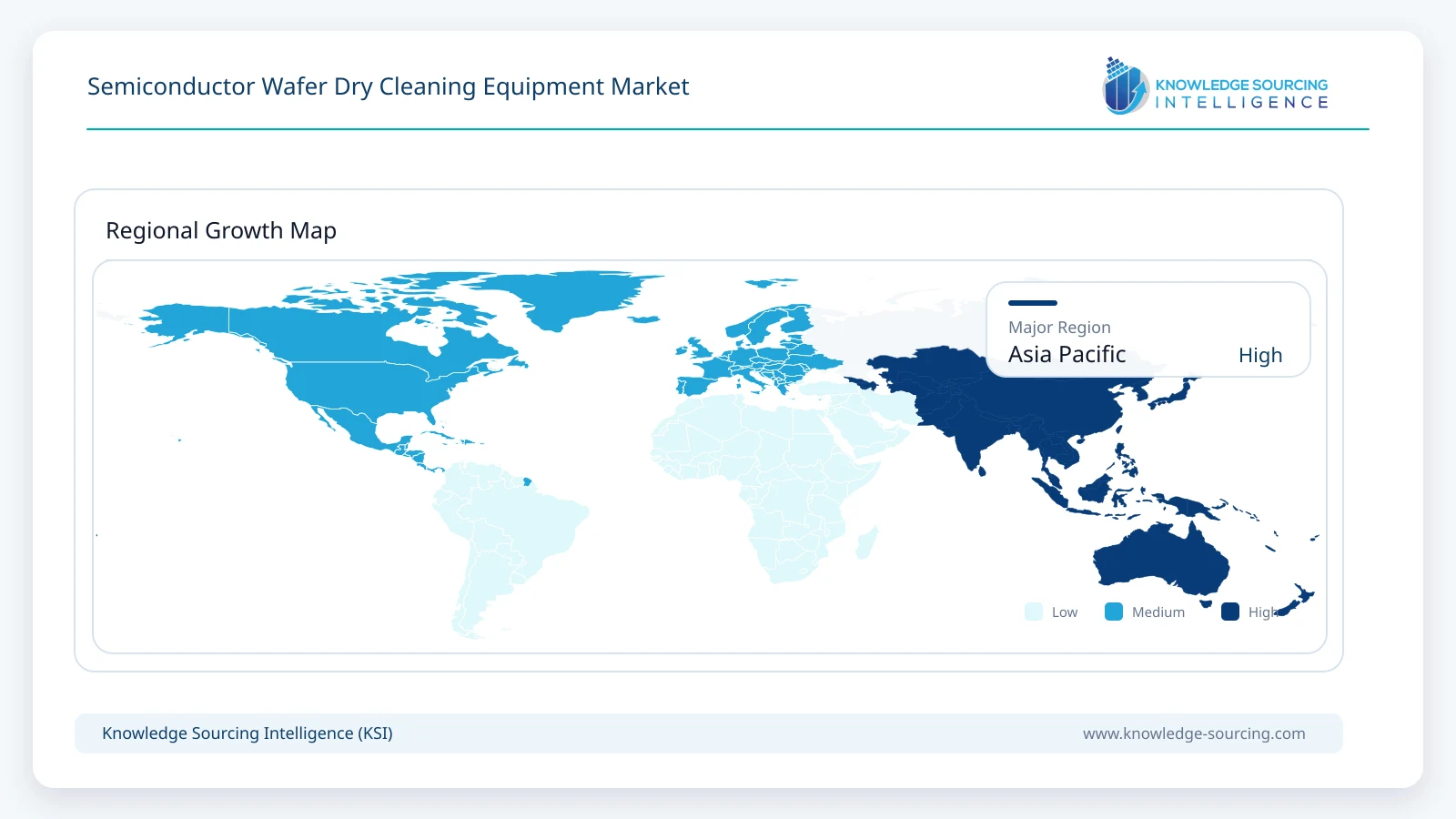
Asia Pacific is the largest market for semiconductor wafer dry cleaning equipment because Taiwan, South Korea, Japan and China contain the majority of advanced logic, DRAM, NAND and packaging capacity. Dry cleaning is particularly relevant in these markets because leading-edge device structures use high-aspect-ratio features, more complex material stacks and advanced bonding flows that require selective, low-damage surface preparation.
South Korea is important through Samsung Electronics and SK hynix as well as PSK, one of the region's specialist dry-process equipment suppliers. PSK links its dry-cleaning technology to the transition into 10 nm-class DRAM and continues to develop next-generation dry-cleaning and surface-treatment equipment. Taiwan contributes through TSMC's leading-edge logic production, HBM and packaging investment, and a growing hybrid-bonding ecosystem. These applications increase the need for pre-bond plasma cleaning, contact cleaning and wafer-edge contamination control.
Japan combines major semiconductor-material and equipment suppliers with advanced image-sensor, power-device, logic and memory production. ULVAC is active in downstream plasma surface preparation and hybrid-bonding research, while Japanese equipment companies provide adjacent cleaning, vacuum and surface-treatment technologies. China adds rapid fab expansion and a growing domestic equipment ecosystem, creating both demand for imported specialist dry-clean platforms and local competition.
North America remains strategically important because Applied Materials is a major supplier of radical-based selective removal and integrated preclean technology, while Bruker supplies cryogenic CO2 wafer-clean systems. Europe is smaller in wafer volume but relevant in MEMS, power semiconductors, compound semiconductors and specialty devices where dry and cryogenic cleaning can provide strong process advantages.
Competitive Landscape
The competitive landscape is more fragmented than the conventional wet-cleaning market because dry cleaning spans several technologies rather than one platform architecture. PSK is a specialist in plasma-based dry strip and dry cleaning for advanced memory and logic. Applied Materials competes through integrated preclean and radical-based selective removal technologies, including Siconi and Selectra process families. Bruker occupies the cryogenic CO2 niche with a field-proven wafer-cleaning installed base.
ULVAC participates in plasma-based surface cleaning and activation for semiconductor and hybrid-bonding processes. Samco-UCP offers remote-plasma wafer cleaning and surface activation up to 300 mm. Plasma-Therm, PVA TePla, Nordson MARCH, YES and other plasma-equipment suppliers participate in adjacent wafer, packaging and bonding surface preparation. SCREEN and Tokyo Electron dominate broader wafer-cleaning equipment but are primarily associated with wet and single-wafer cleaning; their process-development activity remains relevant because dry cleans increasingly need to be co-optimized with upstream and downstream wet-clean steps.
Major companies and ecosystem participants covered: PSK, Applied Materials, Bruker, ULVAC, Samco-UCP, Plasma-Therm, PVA TePla, Nordson MARCH, Yield Engineering Systems, Tokyo Electron, SCREEN Semiconductor Solutions, Lam Research, SPTS Technologies / KLA, Oxford Instruments and regional dry-process equipment suppliers.
Recent Developments
September 2026: Applied Materials published new details on gas-based Selectra Mo selective removal for advanced 3D NAND, highlighting the shift away from liquid-based removal in high-aspect-ratio structures.
September 2026: Bruker presented the WC-2200 cryogenic CO2 dry wafer-cleaning system at SEMICON Taiwan 2026 as part of its semiconductor process portfolio.
May 2026: Applied Materials and SCREEN Semiconductor Solutions announced a joint wafer-cleaning innovation partnership at Applied's EPIC Center.
January 2026: ULVAC presented surface-wave-excited downstream plasma cleaning and activation for hybrid bonding at the IEEE Hybrid Bonding Symposium.
2026: PSK continued development of next-generation dry-cleaning solutions for advanced semiconductor manufacturing and promoted its INTEGER dry-clean platforms.
2026: Samco-UCP continued commercial offering of 300 mm remote-plasma wafer surface-cleaning systems for oxide and organic-residue removal and bonding preparation.
Market Segmentation
By Cleaning Technology
Remote/Downstream Plasma Cleaning
Plasma-Enhanced Selective Cleaning
Radical-Based Gas Cleaning
Cryogenic CO2 Cleaning
Gas-Phase Native-Oxide Removal
Dry Edge and Bevel Cleaning
By Cleaning Objective
Particle Removal
Organic Residue Removal
Native-Oxide Removal
Damaged-Silicon Removal
Polymer and Post-Etch Residue Removal
Surface Activation
By Application
High-Aspect-Ratio Contact Cleaning
DRAM
3D NAND
Gate-All-Around Logic
MEMS and Compound Semiconductors
Hybrid Bonding and 3D Integration
By Wafer Size
300 mm
200 mm
150 mm and Below
By Installation Type
Standalone Single-Wafer Systems
Integrated Cluster Preclean
Batch and Semi-Batch Systems
R&D and Specialty Systems
By Geography
Asia Pacific
Taiwan
South Korea
Japan
China
North America
Europe
Rest of World
Table of Contents
1. EXECUTIVE SUMMARY
1.1. Market Opportunity and Key Findings
1.2. Dry-Cleaning Technology Outlook
1.3. Advanced Logic, Memory and Hybrid-Bonding Demand
2. MARKET OVERVIEW
2.1. Semiconductor Wafer Dry-Cleaning Fundamentals
2.2. Dry versus Wet Cleaning
2.3. Plasma and Radical-Based Cleaning
2.4. Gas-Phase Native-Oxide Removal
2.5. Cryogenic Carbon-Dioxide Cleaning
2.6. Pre-Bond Surface Cleaning and Activation
3. MARKET SIZE AND FORECAST, 2026-2032
3.1. Global Market Revenue
3.2. Annual Growth Analysis
3.3. Equipment, Integration and Service Revenue
4. MARKET BY CLEANING TECHNOLOGY
4.1. Remote/Downstream Plasma Cleaning
4.2. Plasma-Enhanced Selective Cleaning
4.3. Radical-Based Gas Cleaning
4.4. Cryogenic CO2 Cleaning
4.5. Gas-Phase Native-Oxide Removal
4.6. Dry Edge and Bevel Cleaning
5. MARKET BY CLEANING OBJECTIVE
5.1. Particle Removal
5.2. Organic Residue Removal
5.3. Native-Oxide Removal
5.4. Damaged-Silicon Removal
5.5. Polymer and Post-Etch Residue Removal
5.6. Surface Activation
6. MARKET BY APPLICATION
6.1. High-Aspect-Ratio Contact Cleaning
6.2. DRAM
6.3. 3D NAND
6.4. Gate-All-Around Logic
6.5. MEMS and Compound Semiconductors
6.6. Hybrid Bonding and 3D Integration
7. MARKET BY WAFER SIZE
7.1. 300 mm
7.2. 200 mm
7.3. 150 mm and Below
8. MARKET BY INSTALLATION TYPE
8.1. Standalone Single-Wafer Systems
8.2. Integrated Cluster Preclean
8.3. Batch and Semi-Batch Systems
8.4. R&D and Specialty Systems
9. REGIONAL MARKET
9.1. Asia Pacific
9.1.1. Taiwan
9.1.2. South Korea
9.1.3. Japan
9.1.4. China
9.2. North America
9.3. Europe
9.4. Rest of World
10. MARKET DYNAMICS
10.1. Drivers
10.1.1. High-Aspect-Ratio Device Structures
10.1.2. Selective Surface Preparation
10.1.3. Hybrid-Bonding Expansion
10.1.4. Water, Waste and Queue-Time Reduction
10.2. Restraints
10.2.1. Limited Replacement of Wet Cleaning
10.2.2. Plasma-Damage and Chamber-Control Requirements
10.2.3. Throughput Constraints
10.2.4. Fab Integration Complexity
11. COMPETITIVE LANDSCAPE
11.1. Plasma Dry-Clean Specialists
11.2. Selective Removal Platforms
11.3. Cryogenic Cleaning Suppliers
11.4. Hybrid-Bonding Surface Preparation
11.5. Service and Installed-Base Support
12. COMPANY PROFILES
12.1 PSK
12.2 Applied Materials
12.3 Bruker
12.4 ULVAC
12.5 Samco-UCP
12.6 Plasma-Therm
12.7 PVA TePla
12.8 Nordson MARCH
12.9 Yield Engineering Systems
12.10 Tokyo Electron
12.11 SCREEN Semiconductor Solutions
12.12 Lam Research
12.13 KLA Corporation
12.14 Oxford Instruments
13. RECENT DEVELOPMENTS
14. APPENDIX
Navigate
Trusted by the world's leading organizations











