
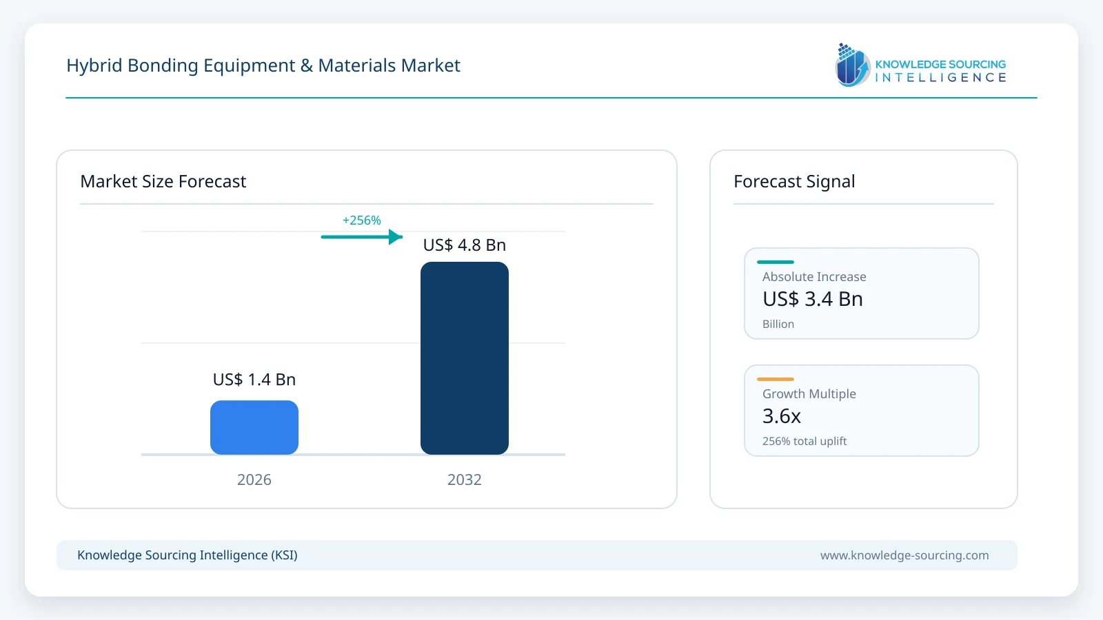
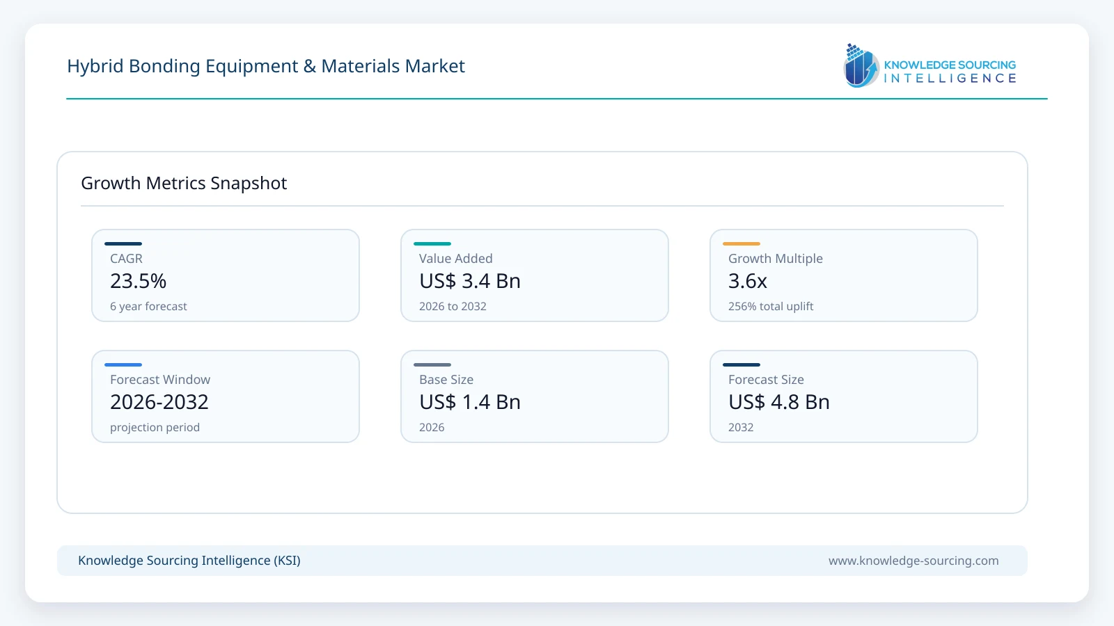
The Hybrid Bonding Equipment & Materials Market is estimated at USD 1.35 billion in 2026 and is projected to reach USD 4.80 billion by 2032, representing a CAGR of 23.5% throughout 2026-2032.
Highlights:
- 1Die-to-wafer hybrid bonding gains momentum for known-good-die chiplets and advanced logic integration.
- 2Wafer-to-wafer bonding remains established in image sensors and selected memory architectures.
- 3AI accelerators and future HBM generations create the strongest new demand for fine-pitch bonding.
- 4Surface preparation, planarization and defect control become as important as bonder placement accuracy.
- 5Asia Pacific leads manufacturing adoption through Taiwan, South Korea and Japan.
Hybrid bonding replaces solder-based microbumps with direct metal-to-metal and dielectric-to-dielectric connections. The process generally requires copper pads to be recessed or controlled within a very tight topography window, dielectric surfaces to be exceptionally flat and clean, and the two wafers or dies to be aligned before room-temperature or low-temperature pre-bonding and subsequent annealing. The interconnect can therefore be scaled to pitches that are difficult to reach economically with conventional solder bumps. The result is higher input/output density, lower parasitic resistance and capacitance, thinner stacks and better use of vertical space.
The manufacturing challenge is that hybrid bonding transfers front-end-like cleanliness and planarization requirements into advanced packaging. Particle contamination that would be tolerable in a conventional assembly process can create voids or open interconnects. Copper dishing, dielectric erosion, surface roughness and wafer bow can reduce bonding yield. Die-to-wafer flows introduce an additional requirement: the system must handle individual known-good dies at high throughput while maintaining sub-micron placement accuracy and preventing particle contamination during pick, transport and placement. This creates demand for integrated equipment chains rather than a single bonding tool.
Wafer-to-wafer hybrid bonding is commercially established in complementary metal-oxide semiconductor image sensors and has been adopted in selected NAND architectures. Die-to-wafer bonding is strategically important for logic chiplets because only tested dies need to be placed on the receiving wafer. TSMC uses direct bonding within its System on Integrated Chips platform for high-density three-dimensional integration, while equipment suppliers are developing platforms for high-throughput die-to-wafer assembly. Memory is the next large opportunity. HBM4 continues to use conventional bump-based assembly, but the industry is preparing hybrid bonding for higher-layer-count HBM4E and HBM5 architectures where stack height, thermal resistance and pitch become more restrictive.
Market Drivers
AI and chiplet architectures require finer die-to-die interconnects
Artificial intelligence processors increasingly combine logic, high-bandwidth memory and specialized chiplets within one package. Electrical performance improves when die-to-die links are shorter and denser, but conventional microbumps consume area and introduce resistance, capacitance and vertical spacing. Hybrid bonding provides direct copper interconnects at much finer pitch, allowing designers to partition large systems without accepting the same interconnect penalty. TSMC reports that its System on Integrated Chips technology has entered volume production for advanced three-dimensional stacking, illustrating that direct bonding has moved beyond laboratory demonstrations into commercial high-performance computing products.
Future HBM generations increase the value of bump-less stacking
High-bandwidth memory is increasing both stack height and input/output density. SK hynix notes that conventional thermo-compression bonding becomes increasingly difficult as pitch approaches approximately 7 micrometers and as stacks move toward 16 to 20 layers. Hybrid bonding removes microbumps and underfill from the vertical interface, reducing stack thickness and interconnect resistance while improving the thermal path between dies. The transition is unlikely to occur uniformly across all HBM products, but HBM4E and HBM5 create a credible volume inflection for hybrid-bonding equipment and process materials.
Process yield depends on surface engineering and metrology
Bond placement accuracy alone cannot guarantee yield. Copper recess, dielectric planarity, surface chemistry, particle count and post-bond void detection determine whether thousands or millions of fine-pitch connections form correctly. Applied Materials is extending chemical mechanical planarization, deposition and copper-processing technology into hybrid-bonding flows, while EV Group combines activation, cleaning, bonding and overlay measurement. As interconnect pitch moves below one micrometer in research programs, process control content per production line rises because manufacturers must detect defects before expensive known-good dies are permanently bonded.
Established sensor and memory applications lower commercialization risk
Hybrid bonding is not dependent on one future AI architecture. Sony and other image-sensor manufacturers have used direct bonding for years, and NAND suppliers have adopted wafer bonding to separate memory-array and peripheral-logic processing. These installed applications give equipment and materials suppliers production experience in surface preparation, alignment and bonding before broader logic and HBM adoption. The resulting process maturity reduces the technology risk for customers qualifying hybrid bonding in advanced packaging lines.
Restraints and Adoption Challenges
Hybrid bonding has a narrower process window than conventional microbump assembly. Particles, surface roughness, copper topography and wafer warpage can cause bond voids or open connections, and defects may only become visible after valuable dies have been committed. Die-to-wafer systems must also balance placement accuracy against throughput, which can raise cost per bonded die during early production ramps. HBM adoption is further constrained by the strong installed base and continued improvement of thermo-compression and molded-underfill processes. For many products, microbumps remain sufficient and cheaper, so hybrid bonding must deliver a clear density, power or stack-height benefit before manufacturers accept the extra process complexity.
Hybrid Bonding Equipment & Materials Market Segment Analysis
By Bonding Format
Wafer-to-wafer hybrid bonding remains the most mature process format because all die positions are bonded simultaneously and the method is already proven in image sensors and selected memory devices. It is most attractive when both wafers have high die yield and compatible die sizes. Die-to-wafer hybrid bonding is expected to expand faster as chiplet architectures, advanced logic and future HBM require known-good dies to be selected and placed individually. Its commercial value is higher per production cell because precision placement, cleaning, inspection and bond alignment must be tightly integrated.
By Product Type
Bonding and precision-placement equipment represents the central capital-equipment category, but the surrounding process stack is becoming more valuable. Surface activation and cleaning systems, chemical mechanical planarization, copper deposition and plating, and sub-micron metrology determine whether the bonder can achieve production yield. Process materials include high-purity cleaning chemistries, dielectric films and precursors, copper plating materials, planarization consumables and surface-conditioning products. Materials suppliers benefit from recurring wafer starts, while equipment suppliers capture larger upfront capital spending during line expansions.
Process Element | Equipment / Material Content | Production Requirement |
Surface planarization | CMP systems, pads, slurries and endpoint control | Extremely low topography variation and controlled copper recess |
Surface preparation | Wet cleaning, plasma activation and high-purity chemistries | Low particle count and bond-ready dielectric surfaces |
Die / wafer alignment | Precision stages, optical alignment and overlay metrology | Sub-micron to nanometer-class placement and overlay control |
Hybrid bonding | Wafer-to-wafer or die-to-wafer bonders | Uniform contact, stable force and controlled thermal cycle |
Copper / dielectric stack | Deposition, plating and dielectric process materials | Repeatable interconnect height and compatible surface chemistry |
Post-bond inspection | Void inspection, acoustic / optical review and metrology | Early detection of incomplete bonds and alignment defects |
Market and Technology Indicators
Indicator | Recent Developments | Market Impact |
Besi hybrid-bonding demand | Besi reported strong 2026 order growth, with particular strength in hybrid bonding, photonics and data-center applications. | Supports a transition from pilot systems toward larger production fleets. |
200 nm wafer-to-wafer pitch | Imec and EV Group demonstrated 200 nm copper interconnect pitch with record overlay accuracy. | Extends hybrid bonding toward very high-density logic and memory stacking. |
Integrated process equipment | Applied Materials expanded CMP, deposition and integrated die-to-wafer bonding capabilities for advanced packaging. | Increases equipment content around the bonder and favors process co-optimization. |
Next-generation HBM | Samsung displayed hybrid copper bonding for future HBM, while SK hynix highlighted hybrid bonding for post-HBM4 scaling. | Creates a large future memory-volume opportunity after current TCB generations. |
3D logic production | TSMC states that 3 nm chip stacking using SoIC entered volume production in 2025. | Confirms direct bonding as a production technology for high-value logic. |
Regional Opportunity
Asia Pacific
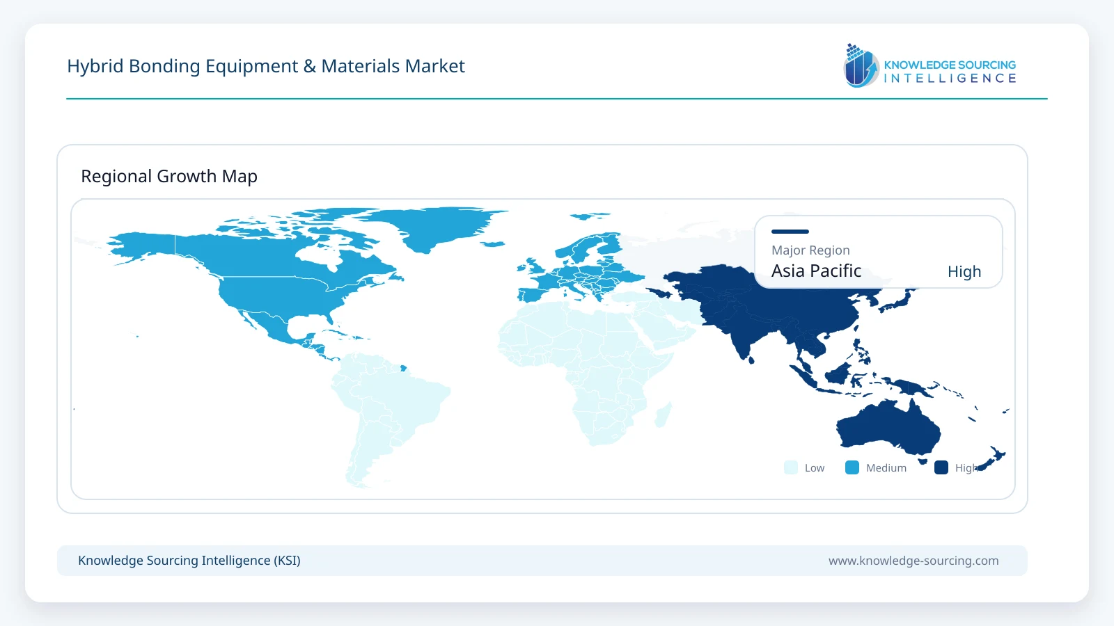
Asia Pacific is the most important production region for hybrid bonding because Taiwan, South Korea and Japan combine leading-edge foundry capacity, memory manufacturing, image-sensor production and advanced packaging. Taiwan is central through TSMC and its System on Integrated Chips and broader 3DFabric ecosystem. The region also contains major outsourced semiconductor assembly and test providers that are adding advanced packaging capacity for AI accelerators and chiplets. This concentration makes Taiwan an early qualification market for die-to-wafer bonders, surface preparation equipment, metrology and associated process materials.
South Korea is the key memory opportunity. Samsung and SK hynix are investing in higher-layer-count HBM and three-dimensional memory architectures, while Samsung has publicly demonstrated hybrid copper bonding for next-generation HBM. SK hynix expects the pressure to move beyond conventional thermo-compression bonding to increase as stack height and input/output density rise. The timing remains dependent on HBM4E and HBM5 product decisions, but qualification work creates equipment and materials demand before full production ramps. South Korea therefore becomes increasingly important for bonders, planarization, cleaning, metrology and copper-interface materials.
Japan contributes both device demand and a deep equipment and electronic-materials ecosystem. Sony is an established user of hybrid bonding in image sensors, while Japanese equipment and materials companies supply cleaning, lithography, chemical, wafer-processing and inspection technologies used in advanced packaging. The country also supports research into high-density three-dimensional integration. China is building advanced packaging capability and has experience with wafer-bonded NAND architectures, while Singapore and Malaysia contribute outsourced packaging capacity and regional equipment support. Together, these markets make Asia Pacific the center of manufacturing deployment even though important equipment suppliers are headquartered in Europe and the United States.
North America contributes strongly through AI processor design, equipment development and materials engineering. Applied Materials is expanding hybrid-bonding process technology, while major processor companies influence die-to-die interconnect requirements. Europe is strategically important through Besi and EV Group, two of the most prominent hybrid-bonding equipment suppliers, as well as research organizations such as imec that help move process capability toward smaller pitch and higher yield.
Competitive Landscape
Competition is concentrated around a small group of equipment suppliers with different process positions. Besi is a leading supplier of high-accuracy die-to-wafer hybrid bonding systems and benefits directly from chiplet, photonics and AI packaging investment. Applied Materials combines surface engineering, chemical mechanical planarization, deposition and bonding through its integrated process strategy and collaboration with Besi. EV Group is particularly strong in wafer-to-wafer bonding, surface activation, cleaning and alignment, and continues to push fine-pitch wafer-bonding performance with imec. ASMPT is developing die-to-wafer hybrid bonding alongside its broader advanced packaging and thermo-compression portfolio.
The competitive field broadens when the complete process flow is considered. SUSS MicroTec participates in wafer bonding and temporary-bonding ecosystems, while Tokyo Electron and SCREEN Holdings supply cleaning and wafer-processing technologies relevant to surface preparation. KLA and Onto Innovation provide inspection and metrology used to monitor overlay, topography and defects. Materials suppliers including Entegris, DuPont, Resonac, JSR and EMD Electronics participate through high-purity chemicals, dielectric and deposition materials, planarization consumables and other process inputs that support advanced packaging and bonding flows.
Differentiation increasingly depends on integrated yield rather than nominal placement accuracy. Customers need a repeatable process from incoming surface preparation through alignment, bonding, annealing and post-bond inspection. Equipment suppliers that can connect process data across these steps, support rapid recipe development and demonstrate stable high-volume throughput have an advantage. Materials vendors must deliver low contamination, tight lot-to-lot consistency and compatibility with increasingly fine copper and dielectric structures. Joint development with foundries, memory manufacturers and research institutes is therefore a central feature of the competitive landscape.
Major companies and ecosystem participants covered: BE Semiconductor Industries (Besi), Applied Materials, EV Group, ASMPT, SUSS MicroTec, Tokyo Electron, SCREEN Holdings, KLA, Onto Innovation, Lam Research, Entegris, DuPont, Resonac Holdings, JSR Corporation and EMD Electronics / Merck KGaA.
Recent Developments
September 2026: ASMPT outlined a four-pillar development framework covering materials, process, equipment and metrology for next-generation bonding technologies, including hybrid bonding.
August 2026: SK hynix identified hybrid bonding as a likely foundational technology for future high-layer-count HBM and other three-dimensional memory products.
July 2026: Besi reported strong first-half growth and highlighted hybrid bonding among the strongest contributors to its order momentum.
June 2026: Applied Materials introduced new CMP, copper-deposition and process-control systems for advanced three-dimensional packaging and hybrid-bonding flows.
May 2026: Imec and EV Group demonstrated wafer-to-wafer hybrid bonding at 200 nm copper interconnect pitch with record overlay accuracy.
March 2026: Samsung showcased hybrid copper bonding technology for next-generation HBM, targeting higher stack counts and lower thermal resistance than conventional bonding.
Hybrid Bonding Equipment & Materials Market Scope:
| Report Metric | Details |
|---|---|
| Total Market Size in 2026 | USD 1.35 billion |
| Total Market Size in 2032 | USD 4.80 billion |
| Forecast Unit | USD Billion |
| Growth Rate | 23.5% |
| Study Period | 2021 to 2032 |
| Historical Data | 2021 to 2024 |
| Base Year | 2025 |
| Forecast Period | 2026 – 2032 |
| Segmentation | Product Type, Bonding Format, Process Material, Application, Customer Type, Geography |
| Companies |
|
Market Segmentation
By Product Type
Die-to-Wafer Hybrid Bonding Equipment
Wafer-to-Wafer Hybrid Bonding Equipment
Surface Activation and Cleaning Equipment
CMP and Surface-Planarization Equipment
Overlay, Inspection and Bond Metrology
Hybrid Bonding Process Materials and Consumables
By Bonding Format
Wafer-to-Wafer Hybrid Bonding
Die-to-Wafer Hybrid Bonding
Die-to-Die and Collective Die Bonding
By Process Material
Dielectric Bonding Materials and Precursors
Copper Plating and Interconnect Materials
CMP Slurries, Pads and Planarization Consumables
Cleaning and Surface-Conditioning Chemistries
Temporary Support and Process Materials
By Application
Logic Chiplets and 3D Logic
High-Bandwidth Memory
CMOS Image Sensors
NAND and Advanced Memory
Co-Packaged Optics and Photonics
Other High-Density 3D Integration
By Customer Type
Foundries and Integrated Device Manufacturers
Memory Manufacturers
Outsourced Semiconductor Assembly and Test Providers
Image-Sensor Manufacturers
Research and Pilot-Line Centers
By Geography
Asia Pacific
Taiwan
South Korea
Japan
China
Southeast Asia
North America
Europe
Rest of World
Table of Contents
1. EXECUTIVE SUMMARY
1.1. Market Opportunity and Key Findings
1.2. Hybrid Bonding Commercialization Outlook
1.3. Principal Equipment and Materials Revenue Pools
2. MARKET OVERVIEW
2.1. Hybrid Bonding Process Architecture
2.2. Copper-to-Copper and Dielectric Bond Interfaces
2.3. Wafer-to-Wafer versus Die-to-Wafer Integration
2.4. Surface Preparation, Planarization and Cleaning
2.5. Overlay, Defect Control and Bond Inspection
3. MARKET SIZE AND FORECAST, 2026-2032
3.1. Global Market Revenue
3.2. Annual Growth Analysis
3.3. Commercialization by Production Stage
4. MARKET BY PRODUCT TYPE
4.1. Die-to-Wafer Hybrid Bonding Equipment
4.2. Wafer-to-Wafer Hybrid Bonding Equipment
4.3. Surface Activation and Cleaning Equipment
4.4. CMP and Surface-Planarization Equipment
4.5. Overlay, Inspection and Bond Metrology
4.6. Hybrid Bonding Process Materials and Consumables
5. MARKET BY BONDING FORMAT
5.1. Wafer-to-Wafer Hybrid Bonding
5.2. Die-to-Wafer Hybrid Bonding
5.3. Die-to-Die and Collective Die Bonding
6. MARKET BY PROCESS MATERIAL
6.1. Dielectric Bonding Materials and Precursors
6.2. Copper Plating and Interconnect Materials
6.3. CMP Slurries, Pads and Planarization Consumables
6.4. Cleaning and Surface-Conditioning Chemistries
6.5. Temporary Support and Process Materials
7. MARKET BY APPLICATION
7.1. Logic Chiplets and 3D Logic
7.2. High-Bandwidth Memory
7.3. CMOS Image Sensors
7.4. NAND and Advanced Memory
7.5. Co-Packaged Optics and Photonics
7.6. Other High-Density 3D Integration
8. MARKET BY CUSTOMER TYPE
8.1. Foundries and Integrated Device Manufacturers
8.2. Memory Manufacturers
8.3. Outsourced Semiconductor Assembly and Test Providers
8.4. Image-Sensor Manufacturers
8.5. Research and Pilot-Line Centers
9. REGIONAL MARKET
9.1. Asia Pacific
9.1.1. Taiwan
9.1.2. South Korea
9.1.3. Japan
9.1.4. China
9.1.5. Southeast Asia
9.2. North America
9.3. Europe
9.4. Rest of World
10. MARKET DYNAMICS
10.1. Drivers
10.1.1. AI and Chiplet Interconnect Density
10.1.2. HBM Stack-Height and Pitch Requirements
10.1.3. Three-Dimensional Logic Integration
10.1.4. Established Sensor and Memory Adoption
10.2. Restraints
10.2.1. Particle and Surface-Defect Sensitivity
10.2.2. Die-to-Wafer Throughput and Placement Cost
10.2.3. Continued Improvement of Thermo-Compression Bonding
10.2.4. Yield Loss from Expensive Known-Good Dies
11. COMPETITIVE LANDSCAPE
11.1. Market Structure and Competitive Intensity
11.2. Die-to-Wafer Bonder Positioning
11.3. Wafer-to-Wafer Bonding and Surface Preparation
11.4. CMP, Cleaning and Process-Control Strategies
11.5. Materials and Consumables Ecosystem
11.6. Foundry, Memory and Research Partnerships
12. COMPANY PROFILES
12.1. BE Semiconductor Industries (Besi)
12.2. Applied Materials
12.3. EV Group
12.4. ASMPT
12.5. SUSS MicroTec
12.6. Tokyo Electron
12.7. SCREEN Holdings
12.8. KLA
12.9. Onto Innovation
12.10. Lam Research
12.11. Entegris
12.12. DuPont
12.13. Resonac Holdings
12.14. JSR Corporation
12.15. EMD Electronics / Merck KGaA
13. RECENT DEVELOPMENTS
14. APPENDIX
Navigate
Trusted by the world's leading organizations











