
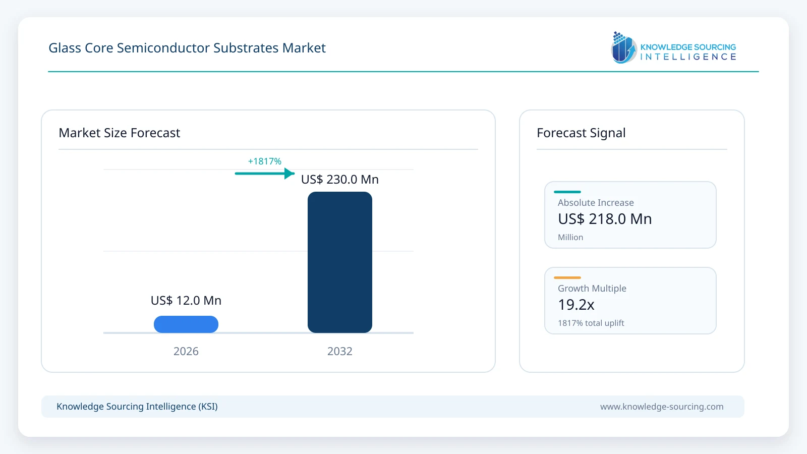
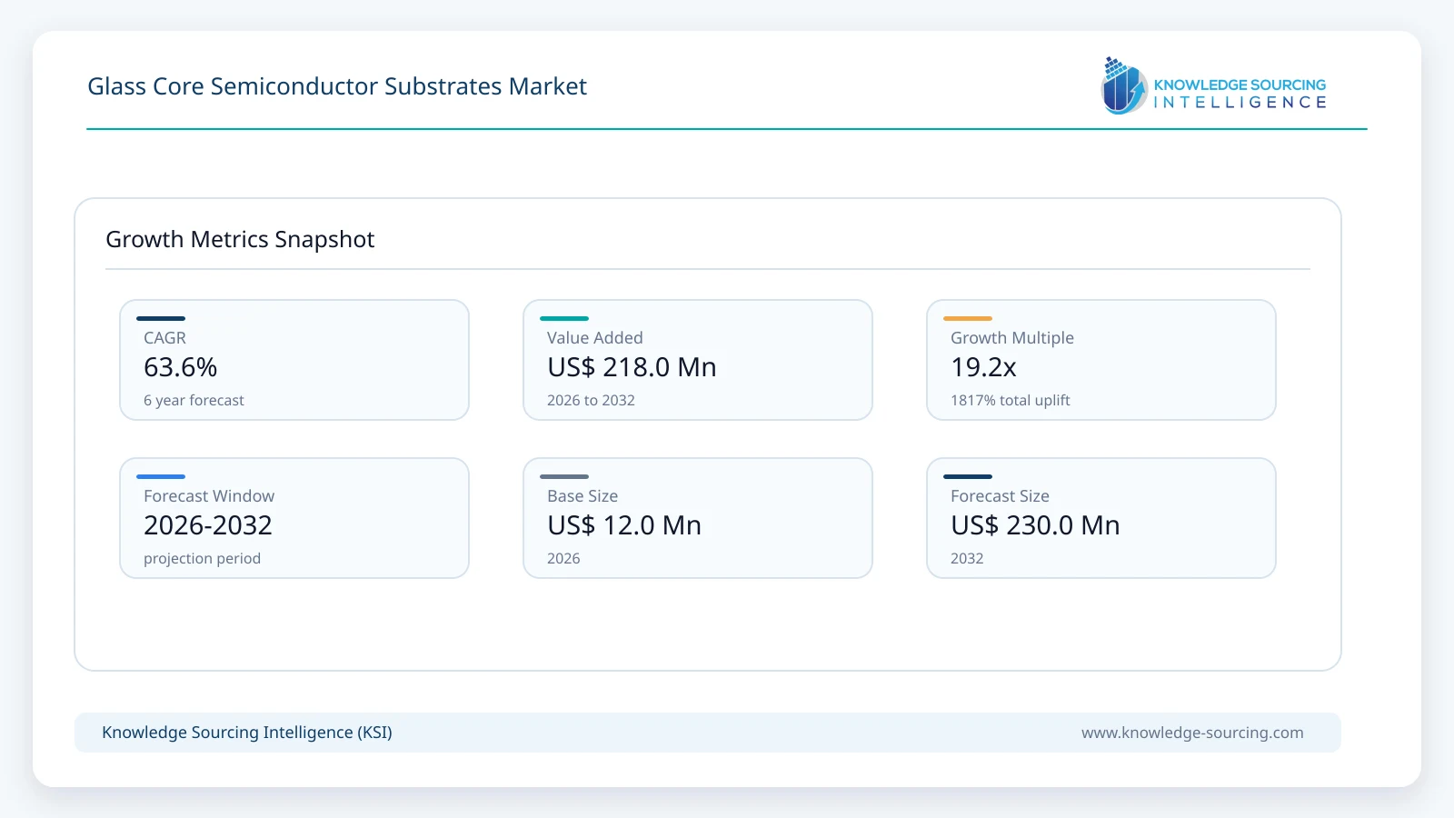
The Glass Core Semiconductor Substrates Market is estimated at USD 12.0 million in 2026 and is projected to reach USD 230.0 million by 2032, representing a CAGR of 63.6% across 2026-2032.
Highlights:
- 1Commercial qualification accelerates as AI packages exceed organic-substrate warpage and routing limits.
- 2Initial volume adoption is expected after 2027 in high-performance computing applications.
- 3Through-glass-via formation and metallization remain critical manufacturing yield and reliability challenges.
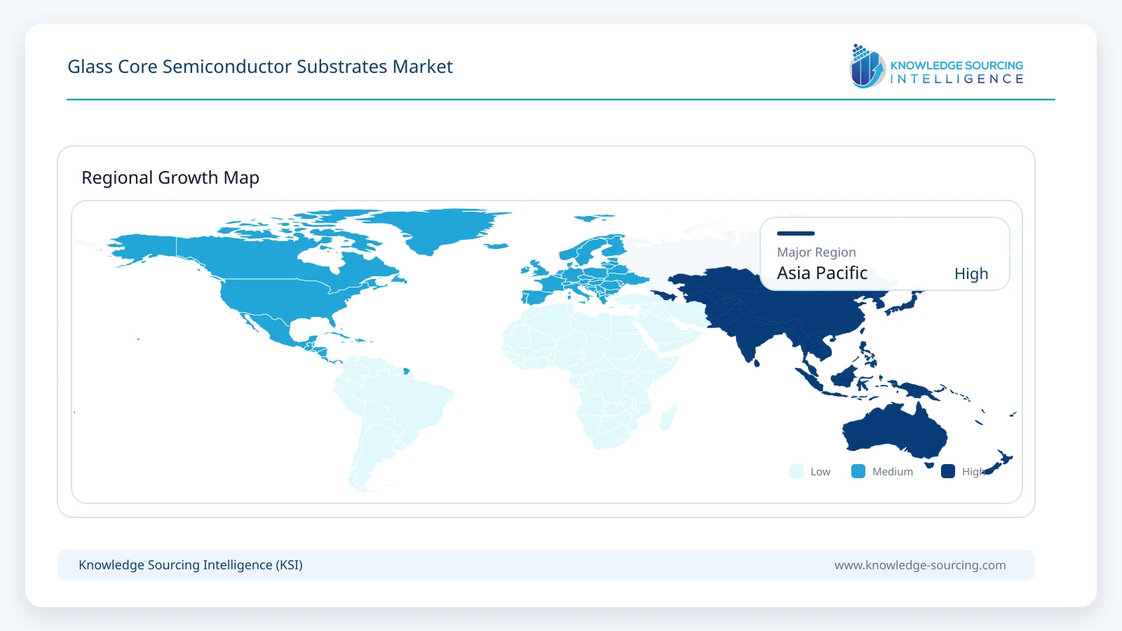
- 4Asia Pacific leads substrate manufacturing depth while North America anchors early commercialization programs.
- 5Glass enables larger package formats, tighter routing and improved dimensional stability for chiplets.
The package substrate sits between the semiconductor package and the printed circuit board, carrying electrical signals and power while providing mechanical support. Conventional high-end substrates typically use organic build-up materials around an organic core. As artificial intelligence packages become larger, the mismatch in thermal expansion between silicon, organic materials and the package structure can increase warpage during assembly and operation. Glass addresses this problem through higher stiffness, better dimensional stability and a coefficient of thermal expansion that can be engineered closer to semiconductor materials.
The electrical case for glass is equally important. A smoother and more stable core can support tighter layer-to-layer registration, finer routing and dense vertical connections through through-glass vias (TGVs). Intel has reported that glass substrates can provide substantially higher interconnect density than organic alternatives and enable larger form-factor packages. Glass also creates opportunities to embed passive components, integrate optical structures and reduce the number of routing layers required for selected package architectures.
Commercialization is not a simple material substitution. Substrate manufacturers need new capabilities for glass handling, precision via formation, seed-layer deposition, copper filling, redistribution layers, build-up lamination, singulation and inspection. Cracking, edge damage, metallization adhesion, via defects and panel handling can reduce yield. The strongest suppliers are therefore developing the glass core together with metallization, build-up processes, inspection, package assembly and design rules rather than selling untreated glass alone.
Market Drivers
AI accelerator packages require larger, flatter and more stable substrates
Artificial intelligence accelerators increasingly combine large logic dies with multiple high-bandwidth memory stacks, chiplets and high-speed input/output interfaces. The resulting package area is substantially larger than a conventional processor package and the number of interconnections rises sharply. Organic cores can distort or warp as package dimensions increase, making fine-pitch assembly more difficult. Glass provides the rigidity and dimensional stability needed to preserve alignment across large substrates, creating a strong adoption case where package yield and electrical performance justify the additional process complexity.
Chiplet integration increases routing density and package-level interconnect requirements
Heterogeneous integration shifts more system-level connectivity into the package. Logic chiplets, memory, accelerators and specialized input/output dies must exchange data across short, high-density connections while receiving stable power. Glass cores can support fine routing, dense TGV structures and embedded components within a mechanically stable platform. The technology therefore complements chiplet architectures that would otherwise require increasingly complex organic routing stacks or large silicon interposers.
Panel-level processing creates a pathway to scale large substrates
Glass can be processed in large rectangular panels, creating a potential manufacturing advantage for high-area package substrates. Panel-level processing can increase the number of units handled per process step and reduce material waste when yields reach commercial targets. Absolics is developing panel-based manufacturing in the United States, while Asian substrate and materials companies are expanding pilot and production capabilities. The economic benefit depends on handling automation, via yield, metallization uniformity and singulation performance improving sufficiently for high-volume manufacturing.
Power delivery and high-speed signaling requirements favor low-loss package platforms
Artificial intelligence and server processors require high current delivery and very high data rates across increasingly complex packages. Glass offers favorable electrical insulation and dielectric characteristics, while its thermal tolerance enables additional package-process flexibility. Intel has also highlighted the potential to integrate inductors, capacitors and optical interconnect structures within glass-based package architectures. These capabilities expand the value proposition beyond mechanical warpage control and position glass as a broader platform for advanced package co-design.
Restraints and Adoption Challenges
Commercial adoption is constrained by manufacturing maturity rather than lack of technical interest. Through-glass-via formation must achieve high density without creating cracks or unacceptable sidewall damage. Copper metallization must adhere reliably to glass, while thermal cycling can introduce stress at material interfaces. Large panels also require specialized handling, inspection and singulation equipment. These challenges can create yield loss and increase cost during early production. Qualification cycles are long because package substrates must meet electrical, mechanical and thermal reliability requirements across the full semiconductor assembly process. Organic substrates also continue to improve, so glass must demonstrate a clear system-level advantage before customers redesign established package platforms.
Glass Core Semiconductor Substrates Market Technology and Application Analysis
By Package Architecture
Glass-core flip-chip ball grid array and large advanced package substrates represent the primary commercialization path because they can replace the mechanically limiting organic core while retaining familiar build-up and assembly concepts. TGV-enabled structures provide vertical connectivity through the glass, while redistribution layers and dielectric build-up layers create the fine horizontal routing needed to connect chiplets and package terminals. Embedded-component glass substrates are a smaller emerging architecture that can integrate passive or active devices to shorten electrical paths and reduce package footprint.
Glass interposer structures remain an adjacent opportunity, particularly for radio-frequency, photonics and high-density heterogeneous integration. In these applications, glass can offer electrical isolation, low loss and dimensional stability while supporting through-glass vias. The distinction between a glass core package substrate and a glass interposer can narrow as package architectures incorporate multiple routing levels, embedded devices and optical functions within the same platform.
By Application
Artificial intelligence accelerators and high-performance computing are the leading commercial targets because these packages combine large area, dense interconnects and strong pressure to reduce power loss. Server central processing units and custom application-specific integrated circuits represent another important opportunity as chiplet designs expand. Radio-frequency and millimeter-wave systems can use glass for low-loss signal transmission and precise dimensional control, while co-packaged optics and photonic integration create a longer-term path where optical and electrical functions are brought closer to compute dies.
Technology and Commercialization Indicators
Indicator | Recent Development | Market Impact |
Interconnect scaling | Intel reports glass can support up to 10x higher interconnect density than organic substrates. | Supports large chiplet complexes and finer package routing. |
Dimensional stability | Intel reports about 50% lower pattern distortion versus organic substrate approaches. | Improves overlay control and large-package assembly yield. |
Industry growth outlook | SEMI projects 67.2% CAGR for glass core substrates from 2028 to 2040. | Indicates a sharp post-qualification commercialization ramp. |
U.S. ecosystem investment | NIST awarded Absolics USD 100 million for glass-core packaging R&D and ecosystem development. | Accelerates process maturity, tooling and domestic supplier development. |
Asian commercialization | Samsung Electro-Mechanics is producing prototypes and targets mass production after 2027. | Creates a second major commercialization path alongside Absolics and Intel. |
Regional Opportunity
Asia Pacific
Asia Pacific has the deepest manufacturing ecosystem for glass core semiconductor substrates because the region combines advanced package-substrate suppliers, specialty glass producers, materials companies, semiconductor assembly providers and major artificial intelligence hardware customers. South Korea is emerging as a central commercialization hub. Samsung Electro-Mechanics operates a pilot line for glass package substrates and is building a glass-core supply structure with Sumitomo Chemical Group and Dongwoo Fine-Chem, while SKC continues to fund Absolics and related glass-substrate development. The region also benefits from established flip-chip ball grid array manufacturing, build-up materials, plating chemistry, precision equipment and substrate inspection capabilities.
Japan contributes specialty glass, materials and substrate-processing expertise. Toppan is developing glass-core flip-chip ball grid array substrates and glass interposers, while companies across the Japanese materials ecosystem supply glass formulations, photoresists, build-up films, plating materials and precision processing equipment. Taiwan remains important through its concentration of advanced packaging, foundry and artificial intelligence accelerator production, creating a natural qualification environment for glass substrate technologies once commercial volumes become available.
The region also benefits from close proximity between substrate manufacturers and package customers. Glass core adoption requires repeated co-development around design rules, TGV pitch, build-up stack, warpage, assembly temperature and package reliability. Locating pilot and production capability close to semiconductor packaging operations can reduce qualification time. This favors Asian manufacturing clusters during the early ramp even as U.S. policy support increases domestic capacity.
North America is the strongest early technology-development and strategic-investment region through Intel and Absolics. Intel has developed glass substrate technology at its advanced packaging operations in Arizona, while Absolics operates its Covington, Georgia facility with federal support. Europe participates mainly through specialty glass, materials, precision equipment and research capabilities rather than large-volume package-substrate production.
Competitive Landscape
Competition is still defined by technology readiness, customer qualification and manufacturing yield rather than installed high-volume capacity. Absolics is one of the most advanced dedicated glass-substrate suppliers and is using its Georgia facility to move from pilot manufacturing toward commercialization. Intel is developing glass substrates as part of its advanced packaging roadmap, focusing on future large-package and high-density computing applications. Samsung Electro-Mechanics is building an integrated glass-core and package-substrate capability and has publicly indicated mass-production plans after 2027.
Toppan participates through next-generation package substrates and glass interposer technologies. Specialty glass suppliers such as AGC, Corning, SCHOTT and Nippon Electric Glass provide material capabilities relevant to substrate flatness, thermal expansion, panel processing and high-frequency performance. Established package-substrate companies including Ibiden, Shinko Electric Industries, Unimicron, Kinsus and AT&S represent potential manufacturing participants as customer demand shifts from organic cores toward hybrid or glass-core platforms.
Competitive differentiation depends on more than the glass material. Suppliers must control via quality, metallization, fine-line redistribution, build-up adhesion, panel warpage, crack prevention, electrical inspection and package reliability. Companies that can provide design support and co-qualification with advanced packaging customers are likely to gain an advantage during the first commercial programs.
Recent Developments
September 2026: Samsung Electro-Mechanics showcased glass substrates and related package technologies for AI accelerators, servers and data-center applications at KPCA Show 2026.
September 2026: SKC approved an additional KRW 281 billion investment in Absolics to accelerate glass-substrate commercialization and reliability evaluation.
May 2026: SEMI and Global Net Corp. released a dedicated glass core substrate market and development report, projecting rapid growth after 2028.
February 2026: SKC announced a KRW 1 trillion rights issue, with approximately KRW 590 billion allocated to Absolics product development.
July 2026: Samsung Electro-Mechanics and Sumitomo Chemical Group signed an agreement to establish a glass-core manufacturing joint venture and target mass production after 2027.
2025: U.S. CHIPS program support for Absolics expanded the domestic glass-core packaging research, manufacturing and supplier ecosystem in Georgia.
Glass Core Semiconductor Substrates Market Scope:
| Report Metric | Details |
|---|---|
| Total Market Size in 2026 | USD 12.0 million |
| Total Market Size in 2032 | USD 230.0 million |
| Forecast Unit | USD Million |
| Growth Rate | 63.6% |
| Study Period | 2021 to 2032 |
| Historical Data | 2021 to 2024 |
| Base Year | 2025 |
| Forecast Period | 2026 – 2032 |
| Segmentation | Package Architecture, Application, Manufacturing Technology, Customer Type, Geography |
| Companies |
|
Market Segmentation
By Package Architecture
Glass-Core FC-BGA Substrates
TGV-Enabled Glass Core Substrates
Embedded-Component Glass Substrates
Glass Interposer and Hybrid Architectures
By Application
AI Accelerators and GPUs
High-Performance Computing and Server CPUs
Custom ASICs and Chiplet-Based Processors
RF and Millimeter-Wave Devices
Co-Packaged Optics and Photonic Integration
Other Advanced Semiconductor Packages
By Manufacturing Technology
Glass Panel Preparation and Handling
Through-Glass Via Formation
Seed Layer and Copper Metallization
Redistribution Layer Formation
Build-Up Dielectric and Fine-Line Routing
Inspection, Singulation and Reliability Testing
By Customer Type
Integrated Device Manufacturers
Fabless Semiconductor Companies
Foundries and Advanced Packaging Providers
Package Substrate Manufacturers
Defense and High-Reliability Electronics
By Geography
Asia Pacific
South Korea
Japan
Taiwan
China
North America
United States
Europe
Rest of World
Table of Contents
1. EXECUTIVE SUMMARY
1.1. Market Opportunity and Key Findings
1.2. Commercialization Timeline
1.3. Technology Readiness and Adoption Outlook
2. MARKET OVERVIEW
2.1. Role of the Package Core in Advanced Semiconductor Packaging
2.2. Organic Core Limitations in Large AI Packages
2.3. Glass Material Properties and Package-Level Benefits
2.4. Through-Glass Via Architecture
2.5. Glass Handling, Metallization and Build-Up Integration
3. MARKET SIZE AND FORECAST, 2026-2032
3.1. Global Market Revenue
3.2. Commercialization Ramp and Volume Adoption
3.3. Pilot, Qualification and Production Transition
4. MARKET BY PACKAGE ARCHITECTURE
4.1. Glass-Core FC-BGA Substrates
4.2. TGV-Enabled Glass Core Substrates
4.3. Embedded-Component Glass Substrates
4.4. Glass Interposer and Hybrid Architectures
5. MARKET BY APPLICATION
5.1. AI Accelerators and GPUs
5.2. High-Performance Computing and Server CPUs
5.3. Custom ASICs and Chiplet-Based Processors
5.4. RF and Millimeter-Wave Devices
5.5. Co-Packaged Optics and Photonic Integration
5.6. Other Advanced Semiconductor Packages
6. MANUFACTURING TECHNOLOGY
6.1. Glass Panel Preparation and Handling
6.2. Through-Glass Via Formation
6.3. Seed Layer and Copper Metallization
6.4. Redistribution Layer Formation
6.5. Build-Up Dielectric and Fine-Line Routing
6.6. Inspection, Singulation and Reliability Testing
7. MARKET BY CUSTOMER TYPE
7.1. Integrated Device Manufacturers
7.2. Fabless Semiconductor Companies
7.3. Foundries and Advanced Packaging Providers
7.4. Package Substrate Manufacturers
7.5. Defense and High-Reliability Electronics
8. REGIONAL MARKET
8.1. Asia Pacific
8.1.1. South Korea
8.1.2. Japan
8.1.3. Taiwan
8.1.4. China
8.2. North America
8.2.1. United States
8.3. Europe
8.4. Rest of World
9. MARKET DYNAMICS
9.1. Drivers
9.1.1. Large AI Package Warpage and Dimensional Stability
9.1.2. Chiplet and High-Density Interconnect Scaling
9.1.3. Panel-Level Manufacturing Economics
9.1.4. Power Delivery and High-Speed Signal Requirements
9.2. Restraints
9.2.1. TGV Yield and Glass-Cracking Risk
9.2.2. Metallization and Interface Reliability
9.2.3. Long Semiconductor Qualification Cycles
9.2.4. Continued Improvement in Organic Substrates
10. COMPETITIVE LANDSCAPE
10.1. Market Structure and Technology Readiness
10.2. Dedicated Glass-Core Substrate Suppliers
10.3. Package-Substrate Manufacturer Strategies
10.4. Specialty Glass and Materials Ecosystem
10.5. Equipment, Inspection and Process Partnerships
11. COMPANY PROFILES
11.1. Absolics
11.2. Intel
11.3. Samsung Electro-Mechanics
11.4. Toppan
11.5. AGC
11.6. Corning
11.7. SCHOTT
11.8. Nippon Electric Glass
11.9. Ibiden
11.10. Shinko Electric Industries
11.11. Unimicron Technology
11.12. Kinsus Interconnect Technology
11.13. AT&S
11.14. Resonac Holdings
11.15. Dai Nippon Printing
12. RECENT DEVELOPMENTS
13. APPENDIX
Navigate
Trusted by the world's leading organizations











