
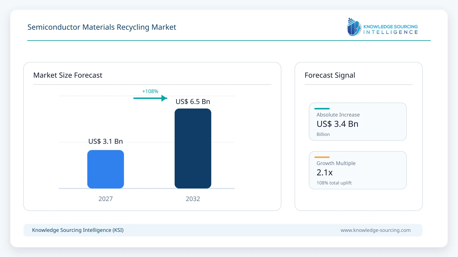
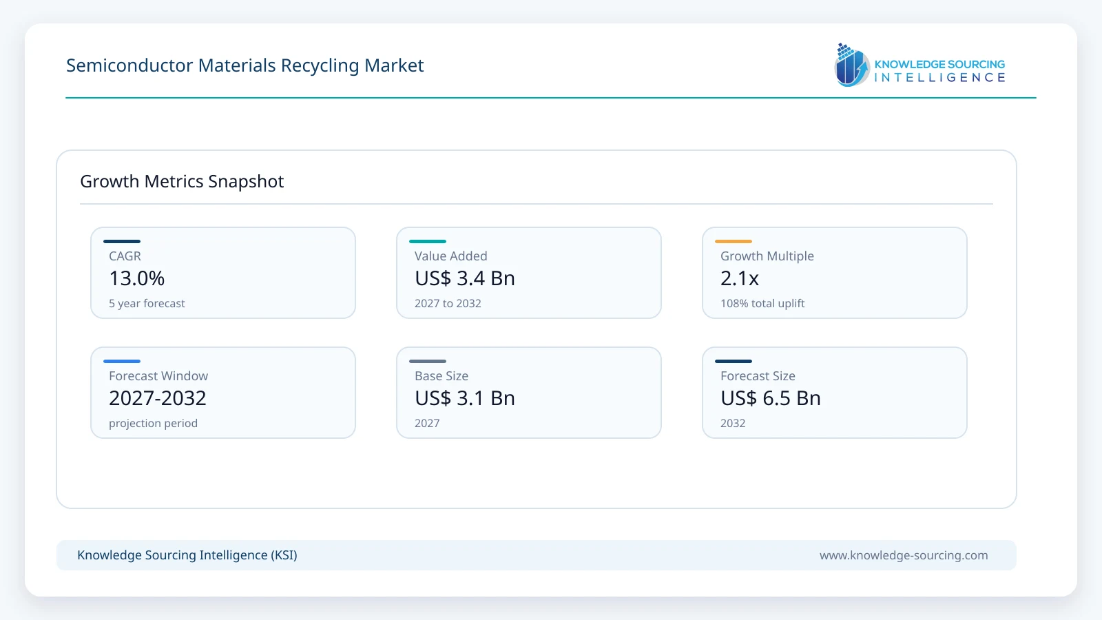
The Semiconductor Materials Recycling Market is estimated at USD 3.10 billion in 2026 and is projected to reach USD 6.45 billion by 2032, representing a CAGR of 13.0% during 2026-2032.
Highlights:
- 1Reclaimed silicon wafers remain the most mature circular-material stream in semiconductor manufacturing.
- 2Closed-loop electronic-grade solvent and chemical recovery is expanding fastest from a smaller revenue base.
- 3Copper, tantalum and precious-metal targets create attractive recovery economics because material value remains high.
- 4Asia Pacific leads demand because wafer fabrication and advanced packaging capacity are concentrated in the region.
- 5Purity, contamination control and qualification determine whether recycled materials can return to semiconductor processes.
Market Overview
Semiconductor recycling differs from conventional industrial recycling because the recovered material frequently has to meet extremely tight purity and contamination specifications. A spent solvent can have value as an industrial chemical after basic recovery, but substantially more value if purification allows it to return to a photolithography or cleaning process. The same distinction applies to metals. Copper, tantalum, ruthenium, gold, silver and other materials recovered from targets, process residues or packaging operations can be sold into general metal markets, or they can be refined and remanufactured into high-purity semiconductor inputs where the qualification burden is much higher.
Wafer reclaim is the most established semiconductor-specific recycling model. Monitor and dummy wafers used for equipment qualification and process control can be stripped, ground or polished, cleaned, inspected and reused repeatedly. RS Technologies states that test wafers account for a meaningful share of wafers entering production lines and that reclaimed wafers are widely used to reduce operating cost. KINIK similarly supplies 8-inch and 12-inch reclaimed wafers for semiconductor fabs. Demand rises with wafer starts because more production steps create more monitor-wafer consumption even when the finished-device wafer itself cannot be reclaimed for its original purpose.
Chemical and target recycling are moving toward closed-loop architectures. TSMC has demonstrated internal and supplier-linked recovery routes for sulfuric acid, IPA, copper sulfate, cobalt-containing waste and sputtering-target materials. Its newer PGME and PGMEA program takes the concept further by purifying spent photolithography solvents back to electronic-grade specifications. This raises the commercial opportunity for separation, purification, analytical testing, logistics and material-regeneration suppliers that can return recovered material to semiconductor production rather than only diverting waste from landfill.
Market Drivers
Fab expansion increases recoverable material volumes
New logic, memory and advanced-packaging capacity increases the absolute volume of process chemicals, monitor wafers, deposition targets and metal-bearing residues moving through semiconductor plants. Advanced manufacturing also uses more process steps, so material consumption does not rise only with wafer starts. Additional deposition, cleaning, lithography and packaging stages create more opportunities to reclaim materials that would otherwise leave the semiconductor value chain. Reclaim providers benefit because high fab utilization provides a steady input stream, while fabs gain a way to reduce virgin-material demand and disposal cost without compromising process control.
High-purity chemical recovery is becoming economically viable
The value proposition improves materially when recovered chemicals can return to semiconductor production. TSMC reported that its PGME and PGMEA recycling technology was validated at Fab 15B and Fab 18A in January 2026 and was scheduled for broader deployment in the second quarter of 2026. After full implementation, the company expects the program to reduce new-liquid procurement by 16,000 metric tons annually. Similar approaches for sulfuric acid, IPA and TMAH show that semiconductor-grade purification is becoming a repeatable operating model rather than an isolated waste-management project.
Critical and precious material recovery supports supply resilience
Semiconductor fabrication and packaging use metals whose value, purity requirements or supply concentration make recovery commercially attractive. Copper, tantalum, ruthenium, gold, silver and other metals are present in sputtering targets, residues, packaging materials and process by-products. Solar Applied Materials Technology operates a closed-loop model for precious and rare metals and provides recycling and refining services for spent tantalum targets and wastes. Heraeus and Umicore operate large precious-metal recycling platforms that can recover high-value metals from electronic and industrial residues. This creates a supply-resilience benefit in addition to the direct recycling revenue.
AI and advanced packaging increase wafer and material intensity
Artificial intelligence accelerators and high-bandwidth memory require advanced packaging flows with more wafer handling, temporary or dummy materials, metallization and process control. TSMC developed a route to convert front-end scrap wafers into dummy dies for Chip on Wafer on Substrate (CoWoS) packaging, with deployment planned across multiple advanced back-end fabs. This type of cross-process reuse expands the addressable market beyond conventional wafer polishing because discarded material from one manufacturing stage can become a qualified input for another semiconductor process. Higher advanced-packaging volumes therefore support both reclaimed-material demand and new recycling technologies.
Restraints and Adoption Challenges
The main constraint is qualification. Semiconductor-grade recycled materials must meet stringent limits for particles, metals, organics, moisture and other contaminants, and a recovery route that works for industrial-grade output may not be acceptable for wafer fabrication. Closed-loop systems also require source segregation so mixed waste does not destroy recovery value. Some materials are generated in volumes too small to justify dedicated recovery infrastructure, while transport and hazardous-material handling can reduce economics. Reclaimed wafers lose thickness with each processing cycle, and not every wafer can be returned to the same application. These limitations keep disposal and lower-grade reuse relevant even as high-value recycling expands.
Segment Analysis
By Recovered Material Stream
Reclaimed wafers represent the largest established semiconductor-specific revenue pool in 2026 because the service is already integrated into fab process-control economics and has specialized global suppliers. The segment includes stripping, polishing, cleaning, inspection and resale or return of monitor and dummy wafers. Chemical recovery is a larger emerging opportunity when several streams are combined, but adoption varies by chemical, fab and local recycling infrastructure.
Electronic-grade solvent and process-chemical regeneration is expected to grow fastest through 2032. The category starts from a smaller base than conventional wafer reclaim and metal recovery but benefits from very large chemical volumes and measurable procurement savings when regenerated material can return to production. Metal and sputtering-target recovery remains highly attractive where precious or critical materials create strong recovery value per kilogram.
Recovered Material Stream | Revenue Contribution | Growth Direction | Primary Semiconductor Recycling Role |
Reclaimed silicon wafers | Largest | Strong | Reuse monitor and dummy wafers for process control and qualification |
Solvents and high-purity process chemicals | High | Fastest | Regenerate IPA, PGME, PGMEA, sulfuric acid, TMAH and related chemicals |
Copper and base-metal process residues | Established | Strong | Recover copper and other metals from plating, sulfate and process streams |
Precious and critical metals / sputtering targets | High-value | Very strong | Recover Ta, Ru, Au, Ag and other high-value target and residue materials |
Scrap wafers and packaging materials | Growing | Very strong | Convert front-end wafer scrap and packaging residues into qualified secondary inputs |
CMP and specialty material streams | Emerging | Strong | Recover selected slurry constituents, abrasives and specialty process materials |
Market and Technology Indicators
Indicator | Current Evidence | Market Impact |
Electronic-grade solvent loop | TSMC validated PGME/PGMEA recovery at Fab 15B and Fab 18A in January 2026. | Raises recycled solvent value by returning material to semiconductor-grade use. |
Reclaimed-wafer capacity | RS Technologies reported favorable demand and accelerated 2026 capacity increases in Japan and Taiwan. | Confirms monitor-wafer recycling is scaling with semiconductor output. |
Advanced-packaging wafer reuse | TSMC developed front-end scrap-wafer conversion into CoWoS dummy dies. | Creates new cross-stage reuse pathways inside semiconductor manufacturing. |
Semiconductor by-product recovery | Veolia acquired Chameleon Industries, which operates four U.S. facilities recovering semiconductor manufacturing by-products. | Expands integrated recovery and chemical circularity services near major U.S. fabs. |
Closed-loop target materials | Solar Applied Materials provides recycling and refining for tantalum-containing spent targets and wastes. | Supports circular supply of high-purity semiconductor target materials. |
Manufacturing waste circularity | Intel applied reuse, recovery or recycling practices to about 69% of manufacturing waste streams in 2025. | Shows large fabs increasingly institutionalize material recovery across operations. |
Regional Opportunity
Asia Pacific
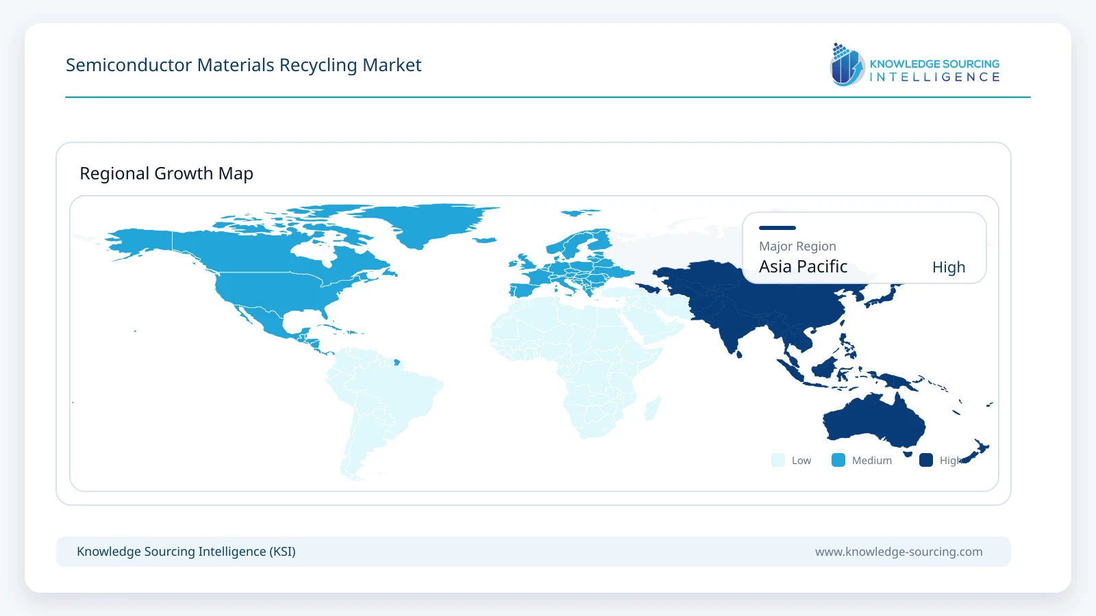
Asia Pacific is the largest opportunity for semiconductor materials recycling because the region contains the greatest concentration of wafer fabrication, memory manufacturing, outsourced semiconductor assembly and test (OSAT), advanced packaging and semiconductor materials production. Taiwan, South Korea, Japan and China generate large and consistent streams of monitor wafers, spent chemicals and target materials. The economics are particularly favorable where reclaim suppliers can operate close to major fabs, reducing transport, handling and qualification time for materials that need controlled logistics.
Taiwan has one of the most developed closed-loop models. TSMC has built internal and supplier-linked systems for sulfuric acid, IPA, copper and cobalt streams, and it is extending recycling into electronic-grade photolithography solvents and scrap-wafer reuse. RS Technologies and KINIK also maintain substantial reclaimed-wafer operations in Taiwan, while Solar Applied Materials combines high-purity target manufacturing with precious- and rare-metal recycling. This creates an ecosystem where wafer reclaim, chemical regeneration and target remanufacturing can all be qualified against demanding semiconductor requirements.
Japan contributes through major wafer, materials and refining companies. RS Technologies is expanding 12-inch reclaim capacity, while Shin-Etsu Chemical gained full ownership of Mimasu Semiconductor Industry and can integrate wafer manufacturing with reclaim capabilities. South Korea adds large memory and logic manufacturing volumes, creating material streams suitable for recovery and reuse. China and Southeast Asia provide additional growth as local fab and packaging capacity expands, although recycling infrastructure and semiconductor-grade qualification depth vary by country.
North America is growing through new fab construction and stronger hazardous-material recovery infrastructure. Veolia’s acquisition of Chameleon Industries added semiconductor by-product recovery facilities in Texas, Oregon and Arizona. Europe contributes through circular-economy policy, specialty refining and high-value materials recovery, particularly precious and critical metals.
Competitive Landscape
The competitive landscape is fragmented because different material streams require different technical capabilities. Wafer reclaim is led by specialist processors with grinding, polishing, cleaning and inspection know-how. RS Technologies, Pure Wafer, KINIK, Mimasu Semiconductor Industry, Phoenix Silicon International, Optim Wafer Services, Silicon Valley Microelectronics and Shinryo compete around wafer diameter, surface quality, turnaround time and proximity to large fabs. Capacity for 300 mm reclaimed wafers is especially important because advanced logic and memory production uses large volumes of monitor wafers.
Chemical and industrial by-product recovery brings in a different supplier group. Veolia combines hazardous-waste handling with semiconductor chemical recovery through Chameleon Industries. Solar Applied Materials operates closed-loop recycling and refining alongside sputtering-target manufacturing. Precious-metal companies including Heraeus Precious Metals and Umicore recover valuable metals from industrial and electronics residues, while TANAKA Precious Metals and DOWA participate across refining and high-purity metals ecosystems. Qualification capability and the ability to return material to a semiconductor-grade application are more important than generic recycling scale alone.
Competitive differentiation increasingly depends on closed-loop yield, purity, analytical control, contamination prevention and logistics integration. Suppliers that can collect segregated material at the fab, regenerate it, verify semiconductor-grade specifications and return it to the same customer capture more value than companies that only convert waste into lower-grade industrial feedstock. Partnerships between fabs, materials suppliers and recyclers therefore become a central part of the market structure.
Major companies and ecosystem participants covered: RS Technologies, Pure Wafer, KINIK, Mimasu Semiconductor Industry / Shin-Etsu Chemical, Phoenix Silicon International, Optim Wafer Services, Silicon Valley Microelectronics, Shinryo Corporation, Veolia / Chameleon Industries, Solar Applied Materials Technology, Heraeus Precious Metals, Umicore, TANAKA Precious Metals, DOWA Eco-System and JX Advanced Metals.
Recent Developments
July 2026: TSMC Nanjing reported a TMAH wastewater-treatment improvement that extended resin life and reduced waste liquid by 387 metric tons annually while increasing regenerated tetramethylammonium chloride (TMAC) concentration.
February 2026: RS Technologies reported strong reclaimed-wafer demand and brought forward a 2026 plant restart while expanding monthly reclaim capacity in Japan and Taiwan.
January 2026: TSMC validated electronic-grade PGME and PGMEA recovery at Fab 15B and Fab 18A, with broader deployment scheduled for the second quarter of 2026.
December 2025: TSMC announced a process that converts front-end scrap wafers into dummy dies for CoWoS advanced packaging, reducing demand for new wafers in this application.
July 2025: Veolia completed the acquisition of Chameleon Industries, adding four U.S. facilities that recover semiconductor manufacturing by-products for beneficial reuse.
2025: TSMC made its Waste Sulfuric Acid Reclaim System 2.0 part of the standard design for new fabs, expanding in-house material regeneration.
Semiconductor Materials Recycling Market Scope
| Report Metric | Details |
|---|---|
| Total Market Size in 2027 | USD 3.10 billion |
| Total Market Size in 2032 | USD 6.45 billion |
| Forecast Unit | Billion |
| Growth Rate | 13.0% |
| Study Period | 2022 to 2032 |
| Historical Data | 2022 to 2025 |
| Base Year | 2026 |
| Forecast Period | 2027 – 2032 |
| Segmentation | Recovered Material Stream, Recycling and Recovery Route, Semiconductor Supply Chain Stage, Commercial Model, Customer Type, Geography |
| Companies |
|
Market Segmentation
By Recovered Material Stream
Reclaimed Silicon Wafers
Solvents and High-Purity Process Chemicals
Copper and Base-Metal Process Residues
Precious and Critical Metals / Sputtering Targets
Scrap Wafers and Advanced-Packaging Materials
CMP and Other Specialty Process Materials
By Recycling and Recovery Route
Direct Wafer Reclaim
Distillation and Solvent Purification
Chemical Regeneration and Ion Exchange
Hydrometallurgical and Electrochemical Recovery
Smelting and Precious-Metal Refining
Remanufacturing and Closed-Loop Material Return
By Semiconductor Supply Chain Stage
Silicon Wafer Manufacturing
Front-End Wafer Fabrication
Advanced Packaging and OSAT
Semiconductor Materials and Target Manufacturing
Equipment Qualification and Process Control
By Commercial Model
Toll Reclaim and Processing Services
Closed-Loop Customer Return Programs
Scrap Purchase and Recovered-Material Resale
On-Site and Co-Located Recovery Systems
Integrated Waste and Material-Management Contracts
By Customer Type
Foundries and Integrated Device Manufacturers
Memory Manufacturers
OSAT and Advanced Packaging Providers
Wafer and Semiconductor Materials Suppliers
Power, Analog and Specialty Semiconductor Manufacturers
By Region
Asia Pacific
Taiwan
Japan
South Korea
China
Southeast Asia
North America
United States
Canada
Europe
Rest of World
Table of Contents
1. EXECUTIVE SUMMARY
1.1. Market Opportunity and Key Findings
1.2. Semiconductor Circular-Materials Outlook
1.3. Principal Revenue Pools
2. MARKET OVERVIEW
2.1. Semiconductor Material Flow and Recovery Architecture
2.2. Reclaimed Wafer Economics and Qualification
2.3. Closed-Loop Chemical Regeneration
2.4. Metal, Target and Process-Residue Recovery
2.5. Cross-Process Reuse in Advanced Packaging
3. MARKET SIZE AND FORECAST, 2026-2032
3.1. Global Market Revenue
3.2. Annual Growth Analysis
3.3. Recycling Revenue by Material Stream
4. MARKET BY RECOVERED MATERIAL STREAM
4.1. Reclaimed Silicon Wafers
4.2. Solvents and High-Purity Process Chemicals
4.3. Copper and Base-Metal Process Residues
4.4. Precious and Critical Metals / Sputtering Targets
4.5. Scrap Wafers and Advanced-Packaging Materials
4.6. CMP and Other Specialty Process Materials
5. MARKET BY RECYCLING AND RECOVERY ROUTE
5.1. Direct Wafer Reclaim
5.2. Distillation and Solvent Purification
5.3. Chemical Regeneration and Ion Exchange
5.4. Hydrometallurgical and Electrochemical Recovery
5.5. Smelting and Precious-Metal Refining
5.6. Remanufacturing and Closed-Loop Material Return
6. MARKET BY SEMICONDUCTOR SUPPLY CHAIN STAGE
6.1. Silicon Wafer Manufacturing
6.2. Front-End Wafer Fabrication
6.3. Advanced Packaging and OSAT
6.4. Semiconductor Materials and Target Manufacturing
6.5. Equipment Qualification and Process Control
7. MARKET BY COMMERCIAL MODEL
7.1. Toll Reclaim and Processing Services
7.2. Closed-Loop Customer Return Programs
7.3. Scrap Purchase and Recovered-Material Resale
7.4. On-Site and Co-Located Recovery Systems
7.5. Integrated Waste and Material-Management Contracts
8. MARKET BY CUSTOMER TYPE
8.1. Foundries and Integrated Device Manufacturers
8.2. Memory Manufacturers
8.3. OSAT and Advanced Packaging Providers
8.4. Wafer and Semiconductor Materials Suppliers
8.5. Power, Analog and Specialty Semiconductor Manufacturers
9. REGIONAL MARKET
9.1. Asia Pacific
9.1.1. Taiwan
9.1.2. Japan
9.1.3. South Korea
9.1.4. China
9.1.5. Southeast Asia
9.2. North America
9.2.1. United States
9.2.2. Canada
9.3. Europe
9.4. Rest of World
10. MARKET DYNAMICS
10.1. Drivers
10.1.1. Fab Expansion and Higher Recoverable Material Volumes
10.1.2. Electronic-Grade Chemical Recovery
10.1.3. Critical and Precious Material Supply Resilience
10.1.4. AI and Advanced-Packaging Material Intensity
10.2. Restraints
10.2.1. Semiconductor-Grade Purity and Qualification Requirements
10.2.2. Source Segregation and Contamination Risk
10.2.3. Uneconomic Low-Volume Material Streams
10.2.4. Wafer Thickness and Reclaim-Cycle Limitations
11. COMPETITIVE LANDSCAPE
11.1. Market Structure and Competitive Intensity
11.2. Wafer Reclaim Capacity and Technology Positioning
11.3. Chemical Recovery and Closed-Loop Semiconductor Services
11.4. Precious and Critical Metal Refining Strategies
11.5. Fab-Supplier-Recycler Partnerships
12. COMPANY PROFILES
12.1. RS Technologies
12.2. Pure Wafer
12.3. KINIK
12.4. Mimasu Semiconductor Industry
12.5. Phoenix Silicon International
12.6. Optim Wafer Services
12.7. Silicon Valley Microelectronics
12.8. Shinryo Corporation
12.9. Veolia
12.10. Solar Applied Materials Technology
12.11. Heraeus Precious Metals
12.12. Umicore
12.13. TANAKA Precious Metals
12.14. DOWA Eco-System
12.15. JX Advanced Metals
13. RECENT DEVELOPMENTS
14. APPENDIX
Navigate
Trusted by the world's leading organizations











