
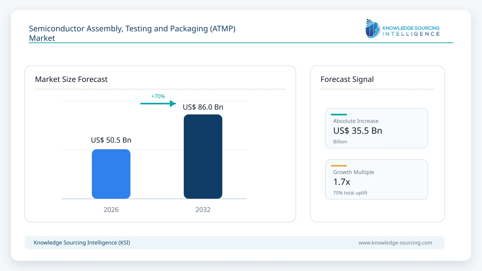
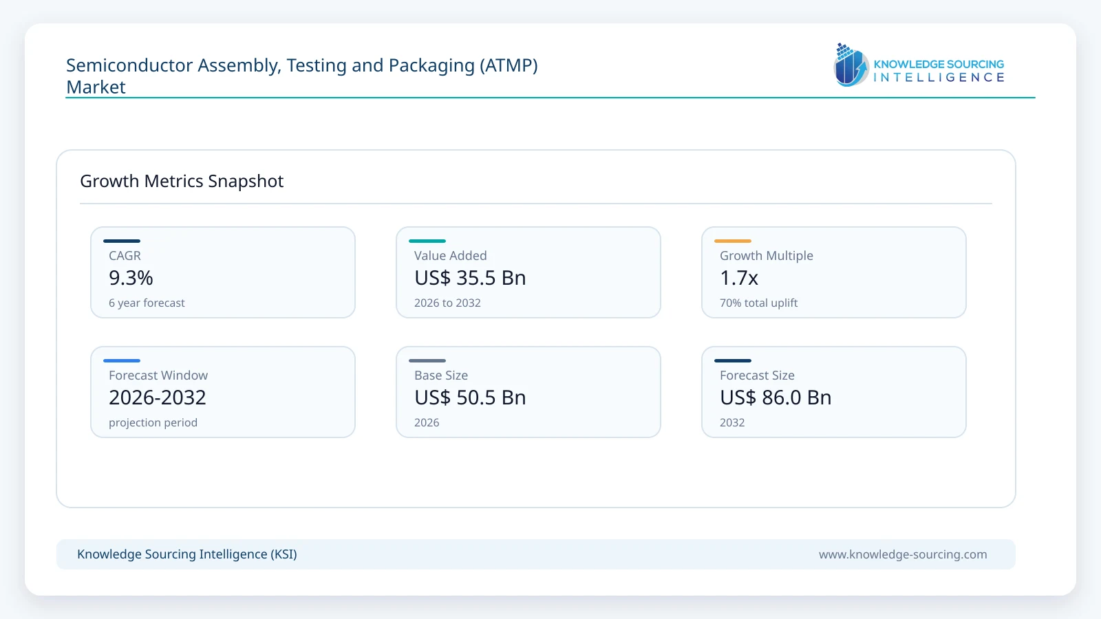
The Semiconductor Assembly, Testing and Packaging (ATMP) Market is forecast to grow at a CAGR of 9.3%, increasing from USD 50.5 billion in 2026 to USD 86.0 billion by 2032.
Highlights:
- 1Assembly and packaging services account for about 67% of 2026 ATMP revenue.
- 2Advanced packaging services are projected to expand at about 13.4% CAGR through 2032.
- 3AI accelerators and HBM increase package complexity and high-end test intensity globally.
- 4Asia Pacific retains the deepest semiconductor assembly, test and packaging manufacturing footprint.
- 5United States and Southeast Asia investments broaden geographic resilience beyond traditional back-end hubs.
Market Overview
ATMP sits between completed wafers and semiconductor devices ready for shipment into electronic systems. A finished wafer must first be electrically screened, singulated and prepared for package assembly. The die is then connected to a package or substrate, protected mechanically and thermally, and tested again under electrical, thermal and reliability conditions. For mainstream analog, microcontroller and power devices, these steps remain highly standardized. For AI processors, networking devices and advanced memory, however, the back-end process increasingly determines bandwidth, power delivery, thermal performance and total system yield.
This shift increases the strategic role of outsourced semiconductor assembly and test providers. Fabless companies can avoid building geographically distributed back-end factories, while integrated device manufacturers can use external capacity for selected products, technologies or peak demand. Large ATMP suppliers now combine conventional packaging lines with wafer-level processing, advanced substrate assembly, system-in-package, heterogeneous integration and increasingly complex test flows. The service relationship therefore moves earlier into product development because package architecture, test strategy and manufacturability must be resolved before high-volume production begins.
Manufacturing location is also becoming more strategic. Taiwan, China, Malaysia, South Korea, Singapore and other Asian production centers remain central to the industry, but customers increasingly want qualified alternatives across several countries. Amkor is building advanced packaging and test capacity in Arizona, while Malaysia and Vietnam continue expanding back-end manufacturing ecosystems. The result is a market where technology capability, geographic resilience and customer qualification are increasingly linked.
Market Drivers
AI and high-bandwidth memory increase advanced packaging content per device
Artificial intelligence accelerators combine large logic dies, high-bandwidth memory stacks, chiplets and high-density interconnects in a single package. The package must support far more interconnect bandwidth and power while maintaining yield across a larger physical area. This increases demand for wafer bumping, redistribution layers, silicon or organic interposers, advanced substrates, flip-chip assembly and fine-pitch integration. ASE is moving panel-level packaging toward production for large AI packages, while Amkor and other OSAT providers are expanding dedicated advanced packaging capacity for accelerated computing.
Semiconductor test requirements become more intensive as device complexity rises
High-value processors and memory devices require more than a basic pass-or-fail final test. Suppliers increasingly perform wafer probe, known-good-die screening, high-speed interface validation, thermal testing, burn-in and system-level test. Multi-die packages create an additional economic incentive to identify defective dies before expensive assembly and to verify the completed package under realistic workloads. ASE is building a dedicated high-tech testing cluster in Kaohsiung, illustrating how advanced test is becoming a capacity category in its own right.
Fabless semiconductor growth supports continued outsourcing of back-end manufacturing
Fabless semiconductor companies typically rely on external manufacturing partners for both wafer fabrication and back-end production. As the number of specialized AI, networking, automotive and edge-computing designs expands, ATMP providers gain from a broader customer base without each customer building its own packaging and test footprint. Large providers can also spread equipment, engineering and qualification costs across many product programs, supporting economically viable access to advanced packaging for customers below hyperscale volumes.
Supply-chain diversification drives new regional assembly and test investment
Customers are increasingly evaluating whether semiconductor back-end capacity is concentrated in too few locations. Government incentives and customer commitments are supporting new capacity in the United States and continued expansion in Malaysia, Vietnam and other Southeast Asian locations. Amkor expanded the planned investment in its Arizona advanced packaging and test campus to approximately USD 12 billion in September 2026, while established Asian suppliers continue to add capacity close to major foundries and electronics manufacturing clusters.
Restraints and Adoption Challenges
ATMP profitability is constrained by cyclical utilization, significant capital requirements and persistent pricing pressure in mature packaging technologies. Advanced packaging equipment and test platforms require large investments before customer volumes are fully visible, while qualification cycles can delay revenue. Yield loss is especially expensive for heterogeneous packages because several high-value dies and memory stacks may be combined in one unit. Customers also expect geographic redundancy without accepting large cost premiums, creating tension between supply-chain diversification and factory utilization. Mature leadframe and wire-bond services remain highly competitive, so suppliers must balance stable high-volume business with faster-growing but more capital-intensive advanced packaging.
Segment Analysis
By Service Type
Assembly and packaging services remain the largest revenue pool in 2026, with an estimated market value of approximately USD 33.8 billion. The segment spans mature leadframe and wire-bond packages through flip-chip ball grid array, wafer-level packaging, fan-out, system-in-package and advanced heterogeneous integration. Mature packages continue to support automotive, industrial, connectivity and consumer devices, while premium revenue increasingly comes from large substrates, chiplets, high-bandwidth memory integration and advanced interconnect structures for AI and high-performance computing.
Advanced packaging is the fastest-expanding technology group within ATMP and is projected to reach approximately USD 35.0 billion by 2032. Growth is driven by 2.5D and 3D integration, chiplets, fan-out, advanced system-in-package and increasingly large substrate-based packages. Semiconductor test remains a substantial separate revenue stream, with growth supported by higher pin counts, faster interfaces, power and thermal validation, burn-in and system-level test. The commercial opportunity therefore shifts toward suppliers that can integrate assembly and testing into a coordinated manufacturing flow rather than provide isolated commodity steps.
ATMP Process and Commercial Role
Back-End Stage | Typical Activities | Commercial Importance |
Wafer preparation and probe | Wafer sort, electrical probe, bumping, redistribution and known-good-die screening | Protects downstream yield and prepares dies for conventional or advanced integration. |
Assembly and package integration | Die attach, wire bond, flip chip, molding, substrate assembly, SiP and heterogeneous integration | Creates the physical, electrical and thermal package architecture used by the final semiconductor. |
Advanced packaging | 2.5D/3D integration, chiplets, fan-out, interposers, advanced substrates and HBM integration | Carries increasing value for AI, HPC, networking and premium mobile processors. |
Final test and burn-in | Electrical test, high-speed interface validation, thermal test, reliability screening and burn-in | Confirms performance and reliability before shipment into systems. |
System-level validation | Module and system testing under representative workloads and environmental conditions | Becomes more important as multi-die packages behave increasingly like integrated systems. |
Market and Technology Indicators
Indicator | 2026 Evidence | Market Relevance |
Global back-end footprint | SEMI and TechSearch International track more than 820 IDM and OSAT assembly and test facilities in the 2026 database. | Shows the scale and geographic breadth of back-end semiconductor manufacturing. |
Amkor revenue momentum | Amkor reported Q2 2026 net sales of USD 1.90 billion, up 26% year-on-year. | Indicates strong demand across computing, automotive and advanced packaging programs. |
U.S. advanced packaging investment | Amkor expanded planned Arizona advanced packaging and test investment to approximately USD 12 billion. | Supports geographic diversification of leading-edge ATMP capacity. |
AI customer commitment | Amkor and NVIDIA announced a USD 1.5 billion multi-year advanced packaging and development agreement. | Links new ATMP capacity directly to next-generation AI infrastructure demand. |
Panel-level scaling | ASE announced an automated 310 mm by 310 mm panel-level packaging line expected to enter production in 2027. | Provides a route to improved area utilization for increasingly large AI packages. |
Taiwan testing expansion | ASE broke ground on a new high-tech testing cluster in Kaohsiung during April 2026. | Demonstrates rising capital intensity and specialization in semiconductor test services. |
Regional Opportunity
Asia Pacific
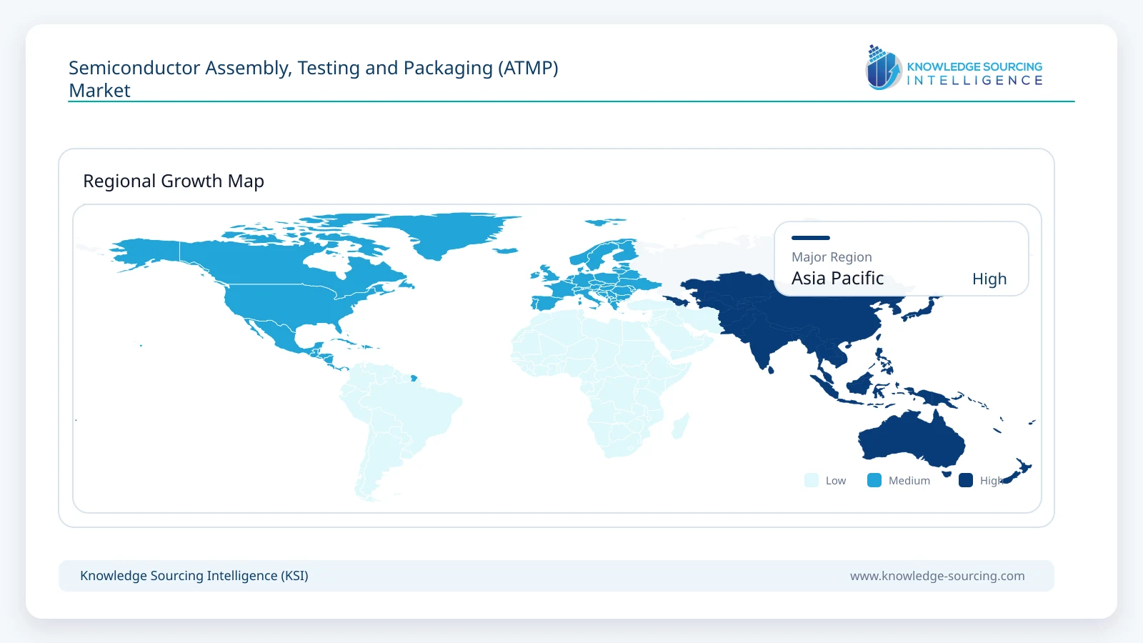
Asia Pacific is the largest regional ATMP market because Taiwan, China, Malaysia, South Korea, Singapore, the Philippines and Vietnam host dense semiconductor and electronics manufacturing ecosystems. Taiwan combines leading foundry capacity with ASE, SPIL and other back-end suppliers, creating a tightly connected environment for advanced package development and volume manufacturing. China contributes major OSAT scale through JCET, Tongfu Microelectronics and other domestic suppliers, while South Korea has deep memory, display and semiconductor manufacturing capability that supports advanced package and test demand.
Malaysia is especially important for geographically diversified assembly and test capacity. Penang has decades of semiconductor back-end experience and continues to attract expansions from global semiconductor manufacturers and ATMP providers. ASE opened an expanded Penang packaging and test facility in 2025 as part of a broader plan to increase its Malaysian manufacturing footprint. Singapore provides high-value semiconductor manufacturing and engineering capability, while Vietnam is scaling assembly, packaging and test operations as global suppliers broaden their Southeast Asian networks.
The region also captures most of the industry learning curve in high-volume manufacturing. Advanced packaging requires close coordination among foundries, substrate vendors, equipment suppliers, material companies and test specialists, so existing clusters have a strong advantage when new technologies enter production. This is why Taiwan remains central even as customers request geographic diversification: new capacity in the United States or Southeast Asia often depends on process transfer and engineering support from established Asian operations.
North America is becoming more important for leading-edge capacity because AI companies and public policy are encouraging domestic advanced packaging. Amkor is developing its Arizona campus with wafer bump, probe, assembly and test capabilities, and its partnerships with NVIDIA and TSMC deepen the connection between U.S. front-end and back-end manufacturing. Europe remains smaller in outsourced ATMP but retains important automotive, power-semiconductor and industrial electronics demand, while new policy programs seek to strengthen regional semiconductor resilience.
Competitive Landscape
The market is led by large outsourced semiconductor assembly and test companies with broad technology portfolios and multi-country manufacturing footprints. ASE Technology Holding combines ASE and SPIL capabilities across conventional assembly, advanced packaging, wafer processing and test. Amkor is differentiated by a large global customer base, advanced packaging depth and major new U.S. capacity. JCET has substantial scale in China and international operations and continues to shift toward advanced packaging and high-performance computing applications.
A second group of companies competes through specialization. Powertech Technology has strong memory packaging and test exposure, while King Yuan Electronics and ChipMOS emphasize semiconductor testing and selected packaging services. Tongfu Microelectronics, UTAC, Unisem, Hana Micron, SFA Semicon and other regional providers serve combinations of analog, automotive, communications, memory, power and consumer devices. Competitive advantage increasingly depends on customer qualification, test capability, advanced substrate handling, yield learning and the ability to ramp new package architectures quickly.
Technology partnerships are becoming more important because leading packages cross traditional company boundaries. Foundries may perform part of wafer-level or advanced packaging, OSAT providers complete assembly and final test, substrate companies supply high-density interconnect platforms, and system companies participate in package co-design. Suppliers that can work within these multi-company manufacturing flows are better positioned as chiplets and heterogeneous integration expand.
Major companies and ecosystem participants covered: ASE Technology Holding, Amkor Technology, JCET Group, Powertech Technology, Tongfu Microelectronics, King Yuan Electronics, ChipMOS Technologies, UTAC Holdings, Unisem, Hana Micron, SFA Semicon, Carsem, Signetics, Walton Advanced Engineering and Orient Semiconductor Electronics.
Recent Developments
September 2026: Amkor announced Phase 2 of its Arizona advanced packaging and test campus, increasing planned investment to approximately USD 12 billion.
July 2026: Amkor and NVIDIA announced a USD 1.5 billion multi-year agreement to expand advanced packaging and test technology for next-generation AI infrastructure.
July 2026: SEMI and TechSearch International released the 2026 Worldwide Assembly & Test Facility Database covering more than 820 facilities globally.
June 2026: TSMC and Amkor announced a long-term partnership intended to accelerate advanced packaging capacity and manufacturing integration in the United States.
May 2026: ASE announced an automated 310 mm by 310 mm panel-level packaging line for AI and high-performance computing, with production targeted for 2027.
April 2026: ASE broke ground on a new high-tech semiconductor testing cluster in Kaohsiung, expanding specialized test capacity.
Semiconductor Assembly, Testing and Packaging (ATMP) Market Scope
| Report Metric | Details |
|---|---|
| Total Market Size in 2026 | USD 50.5 billion |
| Total Market Size in 2032 | USD 86.0 billion |
| Forecast Unit | Billion |
| Growth Rate | 9.3% |
| Study Period | 2021 to 2032 |
| Historical Data | 2021 to 2024 |
| Base Year | 2025 |
| Forecast Period | 2026 – 2032 |
| Segmentation | Service Type, Packaging Technology, Device Type, End User, Business Model, Region |
| Companies |
|
Market Segmentation
By Service Type
Assembly and Packaging Services
Wafer Probe and Sort
Final Test and Burn-In
System-Level Test and Validation
Engineering and Package Development Services
By Packaging Technology
Leadframe and Wire-Bond Packages
Flip-Chip BGA and Laminate Packages
Wafer-Level Packaging
Fan-Out Packaging
System-in-Package
2.5D, 3D and Chiplet Integration
Power and Specialty Semiconductor Packages
By Device Type
Logic and AI Accelerators
Memory and High-Bandwidth Memory
Analog and Mixed-Signal ICs
Power Semiconductors
RF and Connectivity Devices
MEMS, Sensors and Optoelectronics
Microcontrollers and Embedded Processors
By End User
Data Centers and High-Performance Computing
Smartphones and Consumer Electronics
Automotive
Industrial and Power Electronics
Telecommunications and Networking
Aerospace, Defense and Other Applications
By Business Model
Outsourced Semiconductor Assembly and Test Providers
Integrated Device Manufacturer Back-End Services
Foundry-Integrated Advanced Packaging
Hybrid and Strategic Manufacturing Partnerships
By Region
Asia Pacific
Taiwan
China
Malaysia
South Korea
Singapore
Vietnam, Philippines and Rest of Southeast Asia
North America
United States
Mexico and Canada
Europe
Rest of World
Table of Contents
1. EXECUTIVE SUMMARY
1.1. Market Opportunity and Key Findings
1.2. Semiconductor Back-End Manufacturing Outlook
1.3. Principal Revenue Pools
2. MARKET OVERVIEW
2.1. Semiconductor Back-End Manufacturing Flow
2.2. Assembly and Package Integration
2.3. Wafer Probe, Final Test and Burn-In
2.4. Advanced Packaging and Heterogeneous Integration
2.5. OSAT and IDM Back-End Manufacturing Models
3. MARKET SIZE AND FORECAST, 2026-2032
3.1. Global Market Revenue
3.2. Annual Growth Analysis
3.3. Revenue by Assembly, Packaging and Test Service
4. MARKET BY SERVICE TYPE
4.1. Assembly and Packaging Services
4.2. Wafer Probe and Sort
4.3. Final Test and Burn-In
4.4. System-Level Test and Validation
4.5. Engineering and Package Development Services
5. MARKET BY PACKAGING TECHNOLOGY
5.1. Leadframe and Wire-Bond Packages
5.2. Flip-Chip BGA and Laminate Packages
5.3. Wafer-Level Packaging
5.4. Fan-Out Packaging
5.5. System-in-Package
5.6. 2.5D, 3D and Chiplet Integration
5.7. Power and Specialty Semiconductor Packages
6. MARKET BY DEVICE TYPE
6.1. Logic and AI Accelerators
6.2. Memory and High-Bandwidth Memory
6.3. Analog and Mixed-Signal ICs
6.4. Power Semiconductors
6.5. RF and Connectivity Devices
6.6. MEMS, Sensors and Optoelectronics
6.7. Microcontrollers and Embedded Processors
7. MARKET BY END USER
7.1. Data Centers and High-Performance Computing
7.2. Smartphones and Consumer Electronics
7.3. Automotive
7.4. Industrial and Power Electronics
7.5. Telecommunications and Networking
7.6. Aerospace, Defense and Other Applications
8. MARKET BY BUSINESS MODEL
8.1. Outsourced Semiconductor Assembly and Test Providers
8.2. Integrated Device Manufacturer Back-End Services
8.3. Foundry-Integrated Advanced Packaging
8.4. Hybrid and Strategic Manufacturing Partnerships
9. REGIONAL MARKET
9.1. Asia Pacific
9.1.1. Taiwan
9.1.2. China
9.1.3. Malaysia
9.1.4. South Korea
9.1.5. Singapore
9.1.6. Vietnam, Philippines and Rest of Southeast Asia
9.2. North America
9.2.1. United States
9.2.2. Mexico and Canada
9.3. Europe
9.4. Rest of World
10. MARKET DYNAMICS
10.1. Drivers
10.1.1. AI and HBM Advanced Packaging Demand
10.1.2. Rising Semiconductor Test Intensity
10.1.3. Fabless Semiconductor Outsourcing
10.1.4. Geographic Supply-Chain Diversification
10.2. Restraints
10.2.1. Cyclical Capacity Utilization
10.2.2. High Advanced-Packaging Capital Requirements
10.2.3. Yield and Qualification Complexity
10.2.4. Pricing Pressure in Mature Packaging Technologies
11. COMPETITIVE LANDSCAPE
11.1. Market Structure and Competitive Intensity
11.2. Leading OSAT Provider Positioning
11.3. Advanced Packaging and AI Strategies
11.4. Testing and System-Level Validation Strategies
11.5. Regional Capacity and Customer Partnerships
12. COMPANY PROFILES
12.1. ASE Technology Holding
12.2. Amkor Technology
12.3. JCET Group
12.4. Powertech Technology
12.5. Tongfu Microelectronics
12.6. King Yuan Electronics
12.7. ChipMOS Technologies
12.8. UTAC Holdings
12.9. Unisem
12.10. Hana Micron
12.11. SFA Semicon
12.12. Carsem
12.13. Signetics
12.14. Walton Advanced Engineering
12.15. Orient Semiconductor Electronics
13. RECENT DEVELOPMENTS
14. Appendix
Navigate
Trusted by the world's leading organizations











