
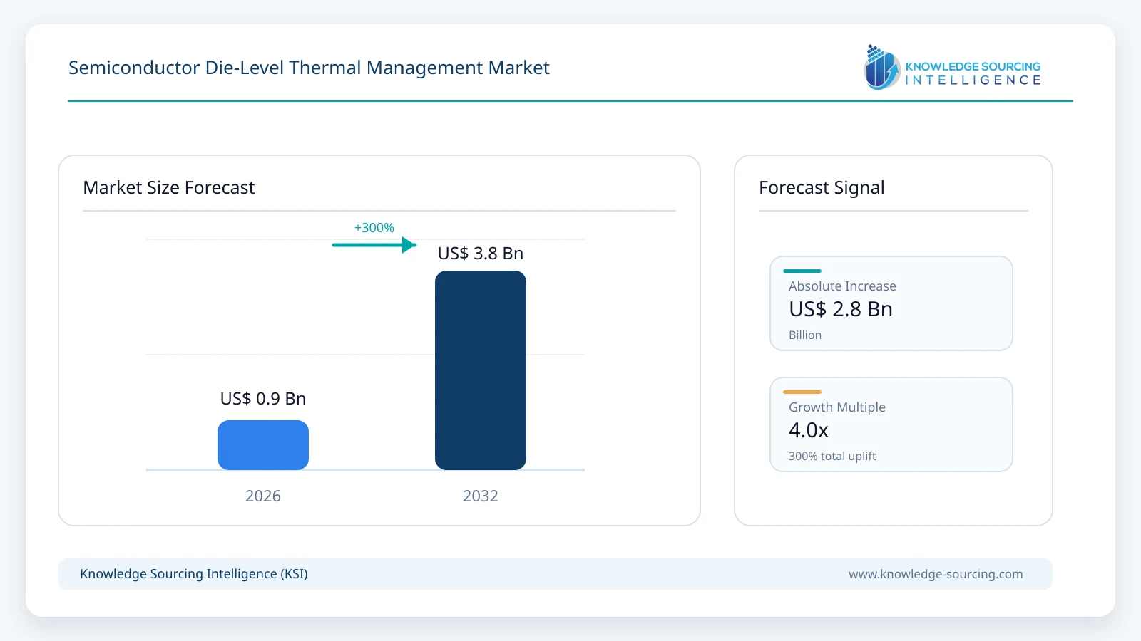
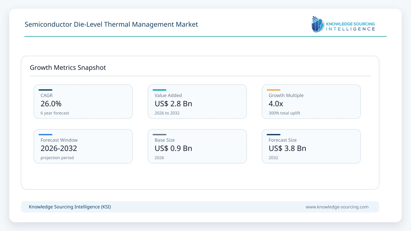
The Semiconductor Die-Level Thermal Management Market is estimated at USD 0.95 billion in 2026 and is projected to reach USD 3.80 billion by 2032, representing a CAGR of 26.0% during 2026–2032.
Key Highlights
• High-conductivity die-attached spreaders provide the largest near-term commercial revenue base across high-power semiconductor packages.
• Embedded microfluidic and in-package liquid cooling are the fastest-moving architectures as AI and HPC heat flux rises beyond conventional package limits.
• Diamond is moving from aerospace and RF niches toward AI processor and advanced-package thermal management.
• Integrated cooling is becoming a co-design issue involving package architecture, bonding, fluid delivery, reliability and manufacturability.
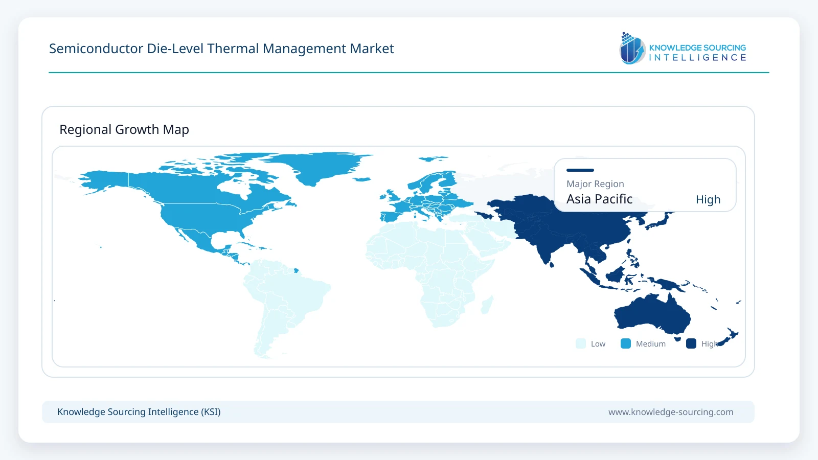
• Asia Pacific is the most important commercialization region because it combines advanced packaging, AI processor manufacturing and a growing supplier base for die-level cooling materials and fabrication.
Market Overview
Conventional semiconductor cooling forces heat through the silicon die, a first thermal interface, a lid or heat spreader, a second interface and finally an external cooler. Each layer adds thermal resistance and spreads heat laterally before it reaches the coolant. That architecture remains adequate for many processors, but it becomes less efficient when large AI packages combine several compute dies and high-bandwidth-memory stacks with very different local heat densities. Die-level thermal management compresses that thermal path by bringing high-conductivity materials or flowing coolant closer to the heat source.
Several architectures are developing in parallel. Diamond and other ultra-high conductivity spreaders can be directly bonded to silicon or integrated into a package to move heat away from hotspots without introducing pumps or fluidic reliability risks. Microchannel coolers place narrow coolant passages in a silicon cap, interposer, package substrate or directly in the back side of the die. Jet-impingement structures direct fluid toward the hottest locations, while manifold microchannels distribute coolant more evenly across large chips. In 2.5D and 3D packages, cooling channels can also be embedded in interposers or intermediate thermal layers to address stacked heat sources.
Manufacturing integration is becoming as important as thermal performance. Microfluidic structures must be fabricated without damaging active devices, weakening thin silicon or creating unacceptable particle and contamination risk. Fluidic ports and seals must survive package assembly, qualification and long-term operation. High-conductivity spreaders require low-void, low-stress bonding to silicon or package materials with very different coefficients of thermal expansion. The commercial market therefore includes not only cooling structures but also fabrication, bonding, laser micromachining and advanced-package integration capabilities.
Market Drivers
AI accelerators are pushing heat removal closer to the junction
AI processors combine high total package power with localized hotspots created by large compute tiles, chiplets and memory interfaces. As thermal design power rises, reducing junction-to-fluid thermal resistance becomes more valuable than simply increasing external coolant flow. This favors solutions that remove one or more package interfaces from the thermal path, including lidless designs, die-bonded spreaders and microfluidic cooling structures integrated into the package or silicon substrate.
2.5D and 3D integration create non-uniform thermal loads
Chiplet packages concentrate logic, cache, input/output and high-bandwidth memory within a limited package footprint. These dies have different power densities and temperature limits, making a single uniform cold plate increasingly difficult to optimize. Localized spreaders, independently controlled cooling zones, microchannels and thermal structures embedded in interposers can target the hottest regions without overcooling the rest of the package. This makes thermal architecture part of floorplanning and package design.
Diamond commercialization improves passive heat spreading
Diamond offers thermal conductivity several times higher than copper while remaining electrically insulating. Historically, cost, film area, bonding yield and integration complexity limited semiconductor use. During 2026, commercial suppliers moved closer to scalable deployment. RFHIC launched packaged-grade CVD diamond spreaders, while CSMH reported GPU and CPU validation of Diamond-on-Silicon composite structures and planned mass production. These developments broaden die-level thermal management beyond liquid cooling alone.
Microfabrication advances make integrated cooling more manufacturable
Microfluidic cooling has long demonstrated strong laboratory performance, but fabrication cost and package integration have limited adoption. TRUMPF is now positioning ultrashort-pulse laser processing for industrial production of microstructures directly within AI-chip stacks, while LPKF is promoting precision laser processing of microfluidic cooling features in glass substrates and interposers. Parallel academic work is showing CMOS-compatible microchannel fabrication below 350°C, improving compatibility with semiconductor back-end processes.
Restraints and Adoption Challenges
The main constraint is manufacturing and reliability risk. Introducing liquid within or directly beside a high-value semiconductor package creates challenges around leakage, corrosion, contamination, pressure drop, seal integrity and field service. Microchannels can also weaken thin silicon or interposer structures and may complicate wafer thinning, bonding and test. Diamond and other high-conductivity materials avoid fluidic risk but remain expensive, require precision bonding and can create thermomechanical stress if package expansion is not managed. These factors mean adoption will be fastest in very high-value AI, HPC, RF and power-electronics applications where additional thermal performance justifies added packaging complexity.
Segment Analysis
By Thermal Architecture
High-conductivity die-attached spreaders and localized heat-spreading structures form the most established commercial category because they can improve junction-to-lid performance without introducing pumps or fluidic infrastructure. Diamond is the most prominent premium material, while copper-diamond composites, graphitic structures and other high-conductivity layers are also being evaluated for advanced packages. Their adoption is strongest where hotspots rather than total package heat limit performance.
Embedded microfluidic and in-package liquid-cooling structures are expected to expand fastest through 2032. They begin from a smaller commercial base but offer the largest reduction in thermal path length. Architectures include microchannels etched or machined into silicon caps, interposers and package substrates; manifold microchannels; jet-impingement structures; and liquid-cooled diamond or glass layers. The fastest adoption is expected in AI accelerators, high-performance computing and selected high-power RF or power-semiconductor packages.
Die-Level Thermal Architecture | Thermal Principle | Primary Semiconductor Use | Commercial Direction |
Diamond / ultra-high-conductivity spreader | Move heat laterally from hotspots with very high thermal conductivity | AI processors, RF, optoelectronics, power devices | Commercializing rapidly from a specialist base |
Silicon microchannel cooler | Flow coolant through channels immediately behind or within the die | AI/HPC processors, research processors | Fast-growing but integration-intensive |
Package-substrate microfluidics | Embed cooling channels in substrate directly beneath the die | Power devices, chiplets, high-power packages | Improves manufacturability versus die-etched cooling |
Interposer-embedded cooling | Use microchannels within a 2.5D interposer or intermediate layer | Chiplet and HBM packages | Strategic for heterogeneous integration |
Jet / impingement cooling | Direct coolant jets toward localized hotspots | Very high heat-flux processors | High performance; fluid delivery remains challenging |
Active multi-zone cooling | Control separate thermal zones for compute and memory | AI chiplets and heterogeneous packages | Emerging with more complex package floorplans |
Market and Technology Indicators
Indicator | Current Evidence | Market Impact |
Integrated chip cooling fabrication | TRUMPF introduced an ultrashort-pulse laser process for producing cooling microstructures directly within AI chip stacks in September 2026. | Moves integrated cooling toward industrial-scale advanced-package manufacturing. |
Commercial diamond spreaders | RFHIC launched DiaFlux CVD diamond heat spreaders in two grades at 1,500 and 1,800 W/m·K in September 2026. | Expands availability of package-ready ultra-high-conductivity materials. |
Diamond-on-silicon production | CSMH reported GPU/CPU validation and planned H2 2026 mass production for its Diamond-on-Si composite heat spreader. | Reduces the gap between diamond research and high-volume AI packaging. |
CMOS-compatible microfluidics | 2026 research demonstrated embedded manifold microchannels above 2,000 W/cm² using fabrication below 350°C. | Shows die-integrated liquid cooling can be compatible with back-end process limits. |
Direct-to-package microfluidics | A 2026 Communications Engineering study demonstrated package-integrated channels dissipating about 625 W/cm². | Offers a scalable path that avoids direct microchannel fabrication in active silicon. |
Interposer cooling | 2026 studies demonstrated microfluidic structures embedded within TSV interposers for 2.5D packages. | Supports localized cooling for chiplets and stacked-memory architectures. |
Regional Opportunity
Asia Pacific
Asia Pacific is the most important commercialization region for die-level thermal management because Taiwan, South Korea, Japan and China combine leading-edge semiconductor fabrication with the largest advanced-packaging ecosystem. AI accelerators, high-bandwidth memory and heterogeneous packages are increasingly manufactured and assembled in the region, placing thermal-management suppliers close to the customers that qualify new materials, microfluidic structures and package-integration processes. SEMICON Taiwan has become a key launch venue for integrated-cooling technologies, including TRUMPF's 2026 microstructure-processing platform.
Taiwan is central through advanced logic and 2.5D/3D packaging, where growing package size and power density make junction-to-coolant thermal resistance a limiting design parameter. South Korea adds high-bandwidth memory, AI packaging and a growing supplier base in diamond and high power semiconductor materials. RFHIC's 2026 DiaFlux launch strengthens the regional supply of CVD diamond heat spreaders, while Korean research teams have demonstrated high-efficiency manifold microchannel cooling compatible with semiconductor processing temperatures.
China is building a domestic ecosystem around thermal materials, advanced packaging and high-power computing. CSMH's Diamond-on-Silicon composite heat spreader is an example of the shift from specialty diamond products toward package-ready solutions for GPU and CPU applications. Japan contributes precision laser, materials and packaging capabilities, while Singapore remains relevant through advanced packaging research and high-density computing programs. The region therefore spans both near-term passive heat-spreading commercialization and longer-term embedded-fluidic architectures.
North America remains a major design and early-adoption market because leading AI processor companies, hyperscalers and thermal-technology startups are concentrated in the United States. Europe contributes strongly through advanced packaging research, laser micromachining and semiconductor equipment, with TRUMPF and European research institutes actively developing integrated cooling fabrication. Commercial adoption outside Asia is likely to remain strongest in AI/HPC, defense, RF and other premium applications before broadening to higher-volume packages.
Competitive Landscape
The competitive landscape is still fragmented across high-conductivity materials, microfluidic cooling, laser and precision fabrication, package integration and direct-chip thermal hardware. RFHIC and specialist diamond suppliers compete in high-conductivity spreaders, while CSMH is positioning Diamond-on-Silicon composites for AI processors. Element Six and other CVD diamond producers provide thermal-grade material used in high-power semiconductor applications. TRUMPF and LPKF address the fabrication layer by enabling fine microstructures in chip stacks, glass substrates and interposers.
Microfluidic and direct-chip specialists include EMCOOL, JetCool and other companies developing coolant delivery close to the package or die. Gemateg is developing active cold plates with separate thermal control zones for chiplet and HBM architectures, while research and packaging organizations such as imec, TNO/CITC and leading OSATs contribute integration know-how that can transition into commercial programs. Competitive advantage increasingly depends on package compatibility, manufacturability, pressure drop, hotspot control, leakage reliability, bonding yield and the ability to integrate thermal structures without disrupting electrical routing or package assembly.
Major companies and ecosystem participants covered: RFHIC, CSMH, Element Six, TRUMPF, LPKF Laser & Electronics, EMCOOL, JetCool, Gemateg, Boyd, Coherent, Morgan Advanced Materials, II-VI / Coherent thermal materials, Akash Systems, Fujipoly and selected advanced-packaging integration partners.
Recent Developments
• September 2026: TRUMPF introduced an ultrashort-pulse-laser application for industrial production of microstructures used in cooling systems integrated directly within AI chip stacks.
• September 2026: RFHIC launched DiaFlux thermal-grade CVD diamond heat spreaders in 1,500 W/m·K and 1,800 W/m·K grades for high-power semiconductor packaging.
• August 2026: CSMH reported packaging and test validation of its Diamond-on-Silicon composite heat spreader for GPU and CPU applications and scheduled mass production for the second half of 2026.
• June 2026: Researchers demonstrated a CMOS-compatible manifold microchannel cooler capable of more than 2,000 W/cm² heat-flux handling with fabrication below 350°C.
• March 2026: TNO, CITC and Delft University researchers published a direct-to-package microfluidic cooling platform demonstrating heat-flux dissipation of approximately 625 W/cm².
• 2026: LPKF expanded its advanced-packaging application portfolio around precision laser fabrication of microfluidic cooling channels in glass substrates and interposers.
Semiconductor Die-Level Thermal Management Market Scope:
| Report Metric | Details |
|---|---|
| Total Market Size in 2026 | USD 0.95 billion |
| Total Market Size in 2032 | USD 3.80 billion |
| Forecast Unit | USD Billion |
| Growth Rate | 26.0% |
| Study Period | 2021 to 2032 |
| Historical Data | 2021 to 2024 |
| Base Year | 2025 |
| Forecast Period | 2026 – 2032 |
| Segmentation | Thermal Architecture, Material Platform, Packaging Architecture, Application, Integration Approach, Geography |
| Companies |
|
Market Segmentation
By Thermal Architecture
Diamond and Ultra-High-Conductivity Heat Spreaders
Silicon Microchannel Coolers
Package-Substrate Microfluidics
Interposer-Embedded Cooling
Jet and Impingement Cooling
Active Multi-Zone Thermal Structures
By Material Platform
CVD Diamond
Silicon
Copper and Copper-Diamond Composites
Glass and Advanced Substrate Materials
Graphitic and Other High-Conductivity Materials
By Packaging Architecture
Monolithic High-Power Packages
2.5D Chiplet Packages
3D Stacked Packages
HBM-Integrated Accelerators
Power and RF Semiconductor Packages
By Application
AI Accelerators
High-Performance Computing
HBM and Advanced Memory
RF and Microwave Semiconductors
Power Semiconductors
Optoelectronics and Photonics
By Integration Approach
Direct-to-Die Bonding
Lid / Cap Integration
Interposer Integration
Package-Substrate Integration
Post-Package Thermal Modules
By Geography
Asia Pacific
Taiwan
South Korea
China
Japan
Singapore and Southeast Asia
North America
Europe
Rest of World
Table of Contents
1. EXECUTIVE SUMMARY
1.1. Market Opportunity and Key Findings
1.2. Die-Level Heat-Flux Outlook
1.3. Integrated Cooling Commercialization
2. MARKET OVERVIEW
2.1. Junction-to-Coolant Thermal Path
2.2. Die-Attached Heat Spreaders
2.3. Embedded and Backside Microfluidic Cooling
2.4. Interposer and Package-Substrate Cooling
2.5. Cooling Co-Design with Chiplet and HBM Packaging
3. MARKET SIZE AND FORECAST, 2026-2032
3.1. Global Market Revenue
3.2. Annual Growth Analysis
3.3. Hardware, Materials and Integration Revenue
4. MARKET BY THERMAL ARCHITECTURE
4.1. Diamond and Ultra-High-Conductivity Heat Spreaders
4.2. Silicon Microchannel Coolers
4.3. Package-Substrate Microfluidics
4.4. Interposer-Embedded Cooling
4.5. Jet and Impingement Cooling
4.6. Active Multi-Zone Thermal Structures
5. MARKET BY MATERIAL PLATFORM
5.1. CVD Diamond
5.2. Silicon
5.3. Copper and Copper-Diamond Composites
5.4. Glass and Advanced Substrate Materials
5.5. Graphitic and Other High-Conductivity Materials
6. MARKET BY PACKAGING ARCHITECTURE
6.1. Monolithic High-Power Packages
6.2. 2.5D Chiplet Packages
6.3. 3D Stacked Packages
6.4. HBM-Integrated Accelerators
6.5. Power and RF Semiconductor Packages
7. MARKET BY APPLICATION
7.1. AI Accelerators
7.2. High-Performance Computing
7.3. HBM and Advanced Memory
7.4. RF and Microwave Semiconductors
7.5. Power Semiconductors
7.6. Optoelectronics and Photonics
8. MARKET BY INTEGRATION APPROACH
8.1. Direct-to-Die Bonding
8.2. Lid / Cap Integration
8.3. Interposer Integration
8.4. Package-Substrate Integration
8.5. Post-Package Thermal Modules
9. REGIONAL MARKET
9.1. Asia Pacific
9.1.1. Taiwan
9.1.2. South Korea
9.1.3. China
9.1.4. Japan
9.1.5. Singapore and Southeast Asia
9.2. North America
9.3. Europe
9.4. Rest of World
10. MARKET DYNAMICS
10.1. Drivers
10.1.1. AI Accelerator Heat Flux
10.1.2. 2.5D and 3D Thermal Coupling
10.1.3. Commercialization of Diamond Heat Spreaders
10.1.4. Advances in Microfabrication and Package Integration
10.2. Restraints
10.2.1. Fluidic Reliability and Leakage Risk
10.2.2. Diamond Cost and Bonding Complexity
10.2.3. Package Qualification Requirements
10.2.4. Manufacturing Yield and Integration Cost
11. COMPETITIVE LANDSCAPE
11.1. Market Structure and Competitive Intensity
11.2. Diamond and High-Conductivity Materials Suppliers
11.3. Microfluidic Cooling Specialists
11.4. Laser and Precision-Fabrication Providers
11.5. Advanced-Packaging Integration Ecosystem
12. COMPANY PROFILES
13. RECENT DEVELOPMENTS
14. APPENDIX
Navigate
Trusted by the world's leading organizations











