
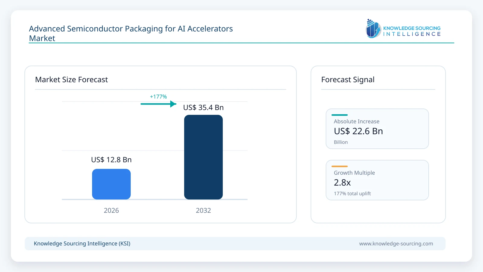
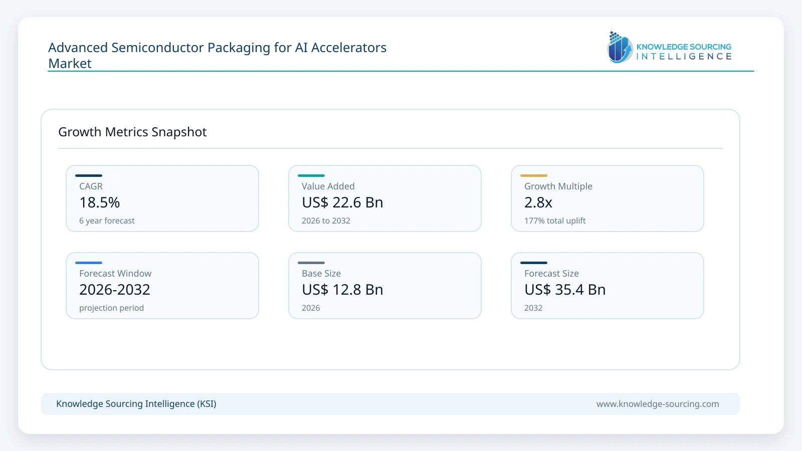
The Advanced Semiconductor Packaging for AI Accelerators Market is estimated at USD 12.8 billion in 2026 and is projected to reach USD 35.4 billion by 2032, representing a CAGR of 18.5% during 2026-2032.
Highlights:
- 12.5D interposer and bridge packages remain the largest AI accelerator packaging architecture in 2026.
- 23D chiplet integration and hybrid bonding are expected to record the fastest commercialization through 2032.
- 3TSMC is moving CoWoS toward 14-reticle-size packages capable of integrating substantially more logic and HBM.
- 4Custom AI ASIC growth broadens demand beyond merchant GPU platforms and increases package-design diversity.
- 5Foundry-integrated packaging leads current high-end AI deployments, while OSAT capacity is expanding rapidly.
- 6Asia Pacific remains the largest manufacturing region through foundry, OSAT, memory and equipment concentration.
- 7U.S. advanced packaging investment is accelerating as AI customers seek geographically diversified capacity.
Market Overview
Advanced packaging is moving from a back-end manufacturing step into a system-scaling technology. A leading AI accelerator package can contain several logic dies, multiple HBM stacks, and tens of thousands of high-speed interconnects across a silicon interposer, redistribution layer, or embedded bridge. The objective is to reduce the physical distance between compute and memory while preserving manufacturability across dies that may use different process nodes. This allows accelerator suppliers to scale compute and memory bandwidth without relying on a single die that becomes uneconomic or impossible to manufacture at the required size.
The dominant 2026 architecture remains 2.5D integration. TSMC CoWoS, Samsung I-Cube, ASE FOCoS, and related platforms place logic and HBM side by side on a fine-pitch interposer or redistribution structure. TSMC states that CoWoS-L and CoWoS-R support package sizes beyond 3.3 times the reticle area, while its 2026 roadmap extends toward much larger multi-reticle formats. These platforms are increasingly paired with local silicon bridges, redistribution layers and advanced package substrates to manage routing, mechanical stress and power delivery as package dimensions expand.
The next transition is toward deeper three-dimensional integration. Intel Foveros Direct uses copper-to-copper hybrid bonding for dense die stacking, while TSMC SoIC and Samsung X-Cube pursue similar vertical integration pathways. Hybrid bonding reduces interconnect pitch and energy per bit compared with conventional microbumps, making it attractive for logic-on-logic, logic-on-base-die and future memory integration. Commercial adoption remains smaller than 2.5D packaging in 2026 because alignment accuracy, surface preparation, known-good-die requirements, and yield learning are demanding, but the technology becomes increasingly important as AI systems require more bandwidth without proportionally increasing package area.
Package scale is also changing manufacturing formats. ASE announced an automated 310 mm square panel-level line supporting FOCoS and FOCoS-Bridge, with production planned for the first half of 2027. A square panel can use area more efficiently than a round wafer for very large packages, potentially reducing cost as interposer size expands. At the same time, glass-core and glass-carrier technologies are being evaluated because they can offer dimensional stability and routing advantages for larger packages. Intel and Lens Technology announced a 2026 collaboration focused on glass-based advanced packaging for AI and data-center workloads.
Market Drivers
AI accelerators are exceeding the practical limits of monolithic dies
Leading-edge logic becomes progressively more expensive as die area increases because a single defect can reduce the yield of an entire large processor. Chiplet architectures allow designers to divide compute, input/output, cache, and other functions across several dies, then reconnect them within one package. Advanced packaging therefore becomes the mechanism that converts multiple smaller dies into a system with near-monolithic performance. Intel is explicitly scaling packages beyond conventional reticle limits using EMIB and Foveros, while TSMC is expanding CoWoS to multi-reticle formats for future AI systems. This shifts a larger share of total semiconductor value into the package-integration layer.
HBM count and bandwidth increase package integration intensity
HBM demand does more than increase memory revenue; it also raises the number of high-density interfaces that must be integrated beside the accelerator. Future AI packages are moving toward more memory stacks, wider interfaces, and larger interposers. TSMC has outlined a 14-reticle-size CoWoS configuration capable of integrating approximately ten large compute dies and twenty HBM stacks by 2028. Each additional logic die, or HBM stack, increases routing density, warpage risk, thermal interaction, assembly steps, and test requirements, supporting higher packaging value even when manufacturing cost per connection declines.
Custom AI silicon broadens the package customer base
The market is no longer driven only by NVIDIA and AMD. Hyperscalers and merchant semiconductor companies are expanding custom AI ASIC programs for training, inference, and networking. These products frequently use HBM and heterogeneous integration but can require different interposer dimensions, substrate layouts, power-delivery solutions and thermal envelopes. A broader set of accelerator architectures increases qualification work and makes packaging capacity more fungible across customers only when suppliers can support multiple design rules and integration flows. This supports investment by foundries and outsourced semiconductor assembly and test providers in flexible advanced-packaging platforms.
Geographic diversification is adding duplicate and incremental capacity
AI customers increasingly want advanced packaging closer to leading-edge wafer fabrication and in more than one geography. Amkor is developing a high-volume U.S. advanced packaging campus in Arizona and expanded the planned investment to approximately USD 12 billion in September 2026. TSMC and Amkor also announced a long-term U.S. partnership, while Intel is expanding advanced packaging capability in New Mexico. These investments do not replace Asian capacity; they add strategic manufacturing options and qualification programs, increasing industry capital intensity and supporting the addressable packaging-services market.
Restraints and Adoption Challenges
Advanced AI packaging carries unusually high yield risk because a finished package can contain several expensive logic dies and multiple HBM stacks. A defect introduced late in assembly can therefore destroy much more value than in a conventional single-die package. Large interposers and substrates also face warpage, thermal-expansion mismatch and power-delivery challenges, while hybrid bonding requires exceptionally flat, clean surfaces and accurate die placement. Capacity expansion can eventually reduce price and lead times, but each new generation introduces fresh process learning. The market is also exposed to architecture changes: alternatives such as local silicon bridges, redistribution-layer interposers, panel-level packaging and wafer-scale systems can shift value between process steps rather than simply increase conventional CoWoS-type revenue.
Segment Analysis
By Integration Architecture
2.5D interposer and bridge integration represents the largest 2026 revenue pool because most high-volume AI accelerators pair logic and HBM side by side on a silicon interposer, redistribution layer or embedded bridge. CoWoS, I-Cube, FOCoS and EMIB-based architectures are established across current AI and HPC platforms. Three-dimensional stacked integration is expected to grow faster through 2032 as hybrid bonding and active base-die approaches move into more logic and memory applications. The transition is gradual because 2.5D architectures continue scaling to much larger package sizes and remain sufficient for many accelerator roadmaps.
By Accelerator Type
GPU accelerators form the largest packaging demand segment in 2026 because they account for the majority of high-end deployed AI compute using multi-die logic and HBM. Custom AI ASICs are expected to expand faster through 2032 as hyperscalers and semiconductor companies develop dedicated training and inference silicon. HPC processors, networking accelerators and other specialized compute devices form a smaller but technically important segment where advanced package architecture can be equally demanding even at lower unit volumes.
Segment | Segment Highlight | Growth Direction | Primary Packaging Logic |
2.5D interposer / bridge | Largest architecture | Strong | Logic plus HBM integration using CoWoS, I-Cube, FOCoS and EMIB-class platforms |
3D / hybrid-bonded integration | Smaller base | Fastest-growing | Fine-pitch die stacking, active base dies and lower-energy die-to-die links |
Fan-out / RDL and panel-level | Emerging at large formats | Accelerating | Reduce interposer cost and improve material utilization for very large packages |
GPU accelerators | Largest accelerator type | Strong | Highest current volume of high-end HBM-equipped AI packages |
Custom AI ASICs | Smaller 2026 base | Fastest accelerator-type growth | Hyperscaler and merchant custom silicon with differentiated package designs |
Technology and Capacity Indicators
Indicator | Revenue Contribution | Market Impact |
TSMC package scaling | 5.5-reticle CoWoS in production; 14-reticle format planned for 2028 | Shows rapid increase in package area, compute-die count and HBM integration |
NVIDIA-Amkor agreement | USD 1.5 billion multi-year advanced packaging and development agreement | Confirms direct AI-customer funding of packaging capacity and technology |
Amkor Arizona expansion | Planned campus investment increased to about USD 12 billion | Adds large U.S. advanced packaging and test capacity |
ASE panel-level packaging | 310 mm x 310 mm automated line planned for production in 1H 2027 | Targets lower cost and better area utilization for large AI packages |
Intel package scaling | Foveros, EMIB and EMIB-T support chiplet integration beyond reticle limits | Broadens foundry-level alternatives for AI heterogeneous integration |
Process equipment investment | Applied Materials launched new CMP, deposition and eBeam systems for AI packaging | Shows yield control and process complexity becoming a larger equipment requirement |
Regional Opportunity
Asia Pacific
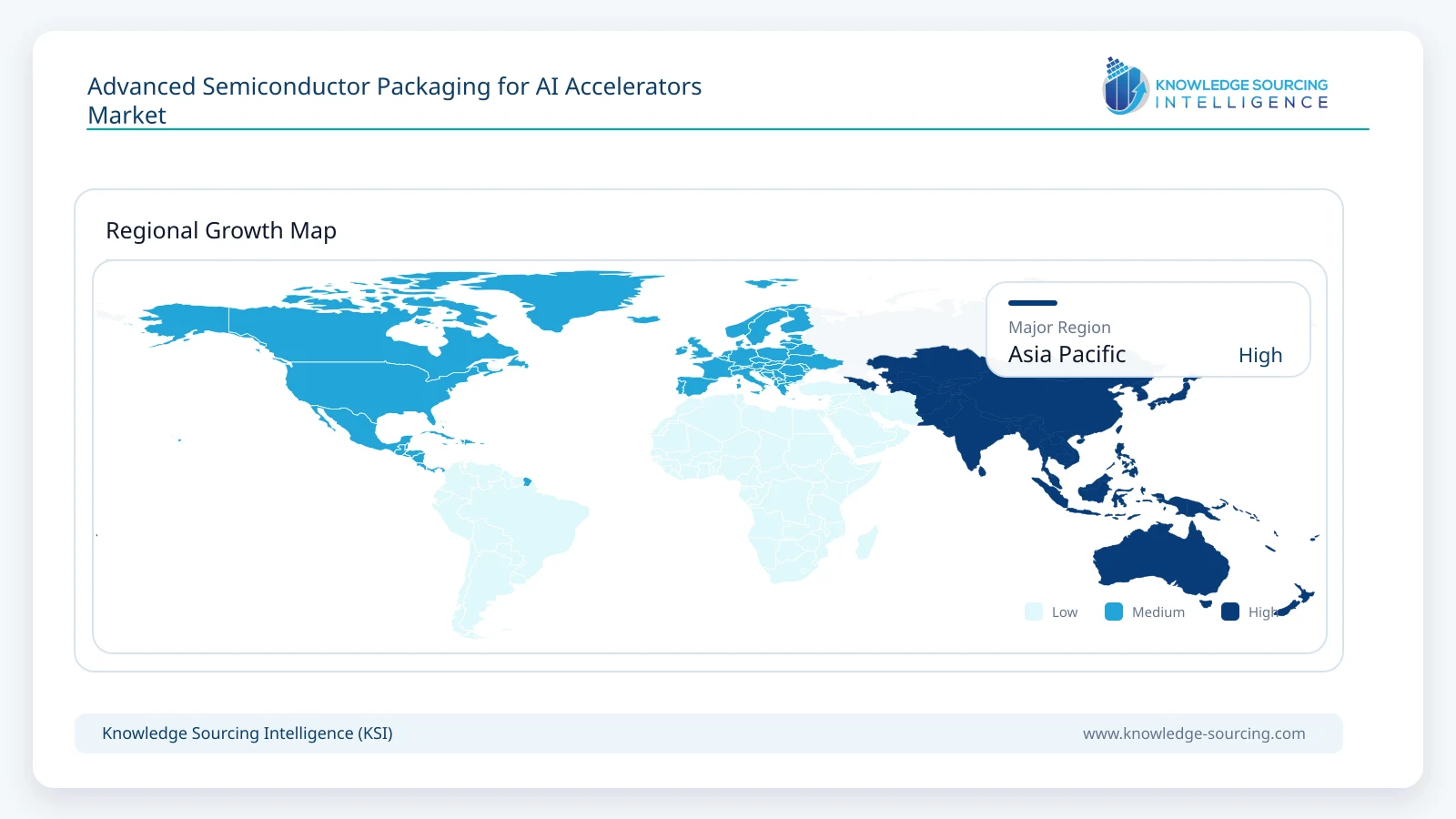
Asia Pacific is the largest market because the region combines leading-edge wafer fabrication, memory manufacturing, advanced packaging, substrate production, and assembly equipment. Taiwan is the center of CoWoS and a major OSAT cluster through TSMC, ASE and Powertech Technology, while South Korea combines HBM production with Samsung advanced packaging and a dense semiconductor materials ecosystem. China has expanded OSAT capacity through JCET, Tongfu Microelectronics and other domestic suppliers, although access to leading-edge tools and customer qualifications varies by process. Japan contributes critical materials, equipment, and emerging glass or advanced-substrate technologies.
Taiwan remains the most important single manufacturing location for high-end AI accelerator packaging because current production combines leading-edge logic wafers, mature CoWoS capacity, major OSAT operations and proximity to substrate and system-assembly partners. TSMC is expanding package dimensions and 3D integration under its 3DFabric platform, while ASE is investing in panel-level packaging and additional high-end test capacity. The concentration creates operating efficiency but also increases customer interest in second-source and geographic diversification.
South Korea has strategic importance through HBM and Samsung's ability to combine memory, foundry and advanced packaging. Samsung Foundry offers 2.5D I-Cube, 2.3D Cube-E and 3D X-Cube pathways, including packages integrating advanced logic with multiple HBM modules. As HBM4 and later generations use more customized logic base dies and wider interfaces, coordination between memory and packaging becomes more important. This creates an opportunity for vertically integrated suppliers while also raising the qualification burden for customers using independent foundry, memory and OSAT partners.
North America is the largest design and end-demand region and is adding manufacturing capacity quickly. Intel operates advanced packaging in New Mexico, Amkor is building its Arizona campus, and U.S. AI-chip companies are increasingly funding packaging capacity directly. Europe remains smaller in production volume but is important in semiconductor equipment, metrology, research and high-performance-computing demand. Through 2032, Asia Pacific is expected to remain dominant in manufacturing even as the United States captures a larger share of incremental high-end packaging investment.
Competitive Landscape
The competitive structure differs from conventional outsourced assembly because foundries now control many of the highest-value AI packaging platforms. TSMC combines leading-edge logic with CoWoS and SoIC, allowing customers to qualify wafer fabrication and packaging within one manufacturing ecosystem. Intel Foundry positions EMIB and Foveros as an open heterogeneous-integration platform, while Samsung combines foundry, memory and package technologies. These integrated suppliers compete on package size, interconnect density, HBM compatibility, yield learning and the ability to coordinate front-end and back-end process roadmaps.
OSAT providers are expanding into higher-value AI packages rather than remaining concentrated in mature assembly. ASE is scaling FOCoS, bridge and panel-level architectures and investing in high-end test. Amkor is using customer-backed U.S. expansion and partnerships with NVIDIA and TSMC to move further into leading AI packaging. JCET, Powertech Technology, Tongfu Microelectronics and other Asian suppliers participate across flip-chip, wafer-level, system-in-package and advanced test, although the most demanding AI accelerator flows remain concentrated among a smaller set of qualified providers.
Equipment suppliers are increasingly strategic participants because package yield depends on processes that resemble front-end wafer manufacturing. Applied Materials is introducing chemical mechanical planarization, deposition and eBeam systems specifically for advanced packaging and HBM. Lam Research is expanding copper deposition and other process technology for 3D interconnects, while Besi and ASMPT participate in high-accuracy die attach and hybrid-bonding equipment. KLA and Onto Innovation provide inspection and metrology needed to control increasingly tight process windows. Competitive advantage therefore depends not only on assembly capacity but on the complete manufacturing ecosystem around bonding, planarization, interconnect formation, inspection and test.
Major companies and ecosystem participants covered: TSMC, ASE Technology Holding, Amkor Technology, Intel Foundry, Samsung Electronics, JCET Group, Powertech Technology, Tongfu Microelectronics, Applied Materials, Lam Research, BE Semiconductor Industries, ASMPT, KLA Corporation, Onto Innovation and Tokyo Electron.
Recent Developments
September 2026: Amkor expanded the planned investment in its Arizona advanced packaging and test campus to approximately USD 12 billion after customer commitments exceeded the initial phase capacity.
July 2026: Intel Foundry detailed how Foveros, EMIB and EMIB-T are being used to scale multi-chip AI packages beyond conventional reticle limits.
July 2026: Intel and Lens Technology announced collaboration on glass-based advanced packaging technologies for future AI and data-center workloads.
July 2026: Amkor and NVIDIA announced a USD 1.5 billion multi-year advanced packaging and development agreement supporting next-generation AI infrastructure.
June 2026: Applied Materials introduced new planarization, deposition and eBeam process-control systems designed for HBM and advanced AI packaging.
June 2026: TSMC and Amkor announced a long-term partnership to accelerate advanced packaging and test capability in the United States.
May 2026: ASE announced the development of an industry-first automated 310 mm × 310 mm panel-level packaging production line, highlighting improved area utilization and material efficiency for complex AI and HPC architectures.
Advanced Semiconductor Packaging for AI Accelerators Market Scope:
| Report Metric | Details |
|---|---|
| Total Market Size in 2026 | USD 12.8 billion |
| Total Market Size in 2032 | USD 35.4 billion |
| Forecast Unit | USD Billion |
| Growth Rate | 18.5% |
| Study Period | 2021 to 2032 |
| Historical Data | 2021 to 2024 |
| Base Year | 2025 |
| Forecast Period | 2026 – 2032 |
| Segmentation | Integration Architecture, Packaging Process, Accelerator Type, Provider Model |
| Companies |
|
Market Segmentation
By Integration Architecture
Redistribution-Layer and Fan-Out Integration
Embedded Silicon Bridge Architectures
Panel-Level and Large-Format Packaging
By Packaging Process
Wafer Bump and Redistribution
Interposer and Bridge Integration
Die Attach and High-Accuracy Placement
Through-Silicon Via Integration
Hybrid Bonding
Assembly, Underfill and Encapsulation
Advanced Test and System Validation
By Accelerator Type
GPU Accelerators
Custom AI ASICs
HPC Processors
Networking and Specialized Accelerators
By Provider Model
Foundry-Integrated Advanced Packaging
Outsourced Semiconductor Assembly and Test Providers
Integrated Device Manufacturers
Packaging Equipment and Process Ecosystem
By Region
Asia Pacific
Taiwan
South Korea
China
Japan
Southeast Asia
North America
United States
Europe
Rest of World
Table of Contents
1. Executive Summary
1.1. Market Opportunity and Key Findings
1.2. Packaging Technology Transition
1.3. Principal Revenue Pools
2. Market Overview
2.1. Evolution from Monolithic Dies to Heterogeneous Integration
2.2. AI Accelerator Package Architecture
2.3. HBM Integration and Package Scaling
2.4. Foundry, OSAT and Equipment Ecosystem
20323.1. Global Market Revenue
3.2. Annual Growth Analysis
3.3. Packaging Value per AI Accelerator
3.4. Capacity Expansion and Yield Effects
4. Market by Integration Architecture
4.2. Redistribution-Layer and Fan-Out Integration
4.3. Embedded Silicon Bridge Architectures
4.5. Panel-Level and Large-Format Packaging
5. Market by Packaging Process
5.1. Wafer Bump and Redistribution
5.2. Interposer and Bridge Integration
5.3. Die Attach and High-Accuracy Placement
5.4. Through-Silicon Via Integration
5.5. Hybrid Bonding
5.6. Assembly, Underfill and Encapsulation
5.7. Advanced Test and System Validation
6. Market by Accelerator Type
6.1. GPU Accelerators
6.2. Custom AI ASICs
6.3. HPC Processors
6.4. Networking and Specialized Accelerators
7. Market by Provider Model
7.1. Foundry-Integrated Advanced Packaging
7.2. Outsourced Semiconductor Assembly and Test Providers
7.3. Integrated Device Manufacturers
7.4. Packaging Equipment and Process Ecosystem
8. Regional Market
8.1. Asia Pacific
8.1.1. Taiwan
8.1.2. South Korea
8.1.3. China
8.1.4. Japan
8.1.5. Southeast Asia
8.2. North America
8.2.1. United States
8.3. Europe
8.4. Rest of World
9. Market Dynamics
9.1. Drivers
9.1.1. Chiplet Adoption and Reticle-Limit Constraints
9.1.2. Rising HBM Count and Bandwidth
9.1.3. Custom AI ASIC Growth
9.1.4. Geographic Capacity Diversification
9.2. Restraints
9.2.1. Yield Risk and Known-Good-Die Requirements
9.2.2. Warpage and Thermal-Mechanical Complexity
9.2.3. Capacity and Equipment Bottlenecks
9.2.4. Rapid Architecture Transitions
10. Technology Outlook
10.3. Panel-Level Packaging
10.4. Glass-Core and Glass-Carrier Technologies
10.5. Advanced Power Delivery and Thermal Integration
10.6. Package-Level Co-Design and Digital Twins
11. Competitive Landscape
11.1. Value Chain
11.2. Foundry Packaging Platforms
11.3. OSAT Advanced Packaging Platforms
11.4. Equipment and Process Control
11.5. Capacity Expansion and Customer Partnerships
12. Company Profiles
12.1. TSMC
12.2. ASE Technology Holding
12.3. Amkor Technology
12.4. Intel Foundry
12.5. Samsung Electronics
12.6. JCET Group
12.7. Powertech Technology
12.8. Tongfu Microelectronics
12.9. Applied Materials
12.10. Lam Research
12.11. BE Semiconductor Industries
12.12. ASMPT
12.13. KLA Corporation
12.14. Onto Innovation
12.15. Tokyo Electron
13. Recent Developments
14. Appendix[Write methodology here]The market is analyzed using top-down and bottom-up approaches...
Navigate
Trusted by the world's leading organizations











