
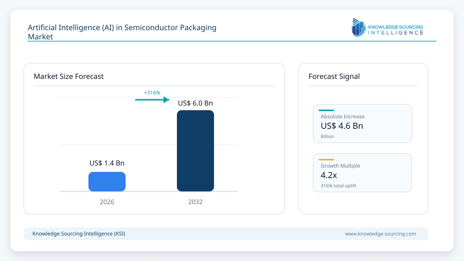
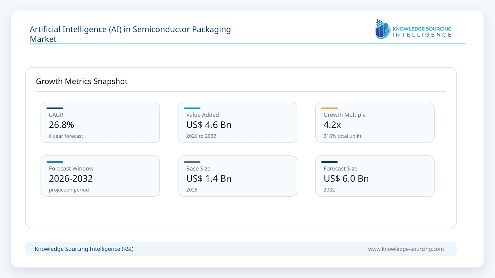
The Artificial Intelligence (AI) in Semiconductor Packaging Market is estimated at USD 1.45 billion in 2026 and is projected to reach USD 6.03 billion by 2032, representing a CAGR of 26.8% during 2026-2032.
Highlights:
- 1AI-enabled inspection and defect classification represent the largest commercial application in 2026.
- 2Agentic package-design and multiphysics workflows are the fastest-growing application through 2032.
- 3Hybrid bonding and chiplet integration increase the value of automated defect and yield intelligence.
- 4Asia Pacific leads deployment through its concentration of foundry, OSAT and packaging capacity.
- 5AI adoption is shifting from isolated models toward closed-loop, semiconductor-specific manufacturing platforms.
Market Overview
Semiconductor packaging produces unusually rich manufacturing data because each package can pass through wafer thinning, redistribution, bumping, bonding, molding, singulation, inspection and multiple test stages before shipment. Advanced packages add more layers of data from interposers, through-silicon vias, microbumps, hybrid bonds, chiplets and high-bandwidth memory stacks. The value of AI comes from correlating these measurements across process steps rather than optimizing one machine in isolation. Packaging companies can use prior inspection, metrology and test results to predict downstream failures, alter sampling plans, refine process windows and prevent known-bad die from consuming additional high-value assembly capacity.
Inspection is the most mature AI application. KLA's DefectWise platform and ICOS inspection systems use AI and deep-learning classification to improve defect binning, while Onto Innovation's TrueADC combines deep learning with real defect libraries and reports more than 70% reduction in manual review. These tools are especially relevant in advanced packaging because defect counts rise rapidly with bump density and package complexity, while the cost of incorrectly rejecting or accepting a die increases once several high-value components are integrated into one package.
Design automation is becoming a second major revenue pool. Cadence AuraStack coordinates AI agents across package planning, implementation, constraints and multiphysics analysis, while Synopsys is integrating AI-powered design flows with 3DIC Compiler and system-level thermal, electromagnetic and power-integrity analysis. Siemens EDA is similarly developing AI-native workflows for 3D integrated-circuit design and long-running self-verifying engineering agents. The commercial opportunity therefore extends from factory analytics into the front end of package architecture, where AI can reduce design iterations before expensive hardware is built.
Market Drivers
Advanced packaging increases inspection and process-control complexity
Hybrid bonding, chiplet assembly and high-density redistribution layers operate with smaller process windows than conventional packaging. A particle, alignment error or microbump defect that might have been tolerable in an older package can destroy yield in a multi-die assembly containing expensive logic and memory. Applied Materials introduced advanced-packaging eBeam metrology and defect-review systems in 2026 specifically because feature dimensions and package complexity are moving beyond conventional optical-control approaches. AI-based classification adds value by converting the resulting inspection volume into actionable defect categories and faster yield learning.
Packaging data volume is outgrowing manual engineering workflows
Manufacturing and test data are expanding as more package steps become digitally monitored. PDF Solutions reported that advanced packaging has contributed to a sixfold increase in the amount of manufacturing and test data that some semiconductor companies need to analyze since 2022. AI and machine learning allow engineers to correlate assembly, inspection and test information across millions of measurements without manually building every analysis path. This supports automated root-cause identification, anomaly detection and predictive quality decisions.
AI-assisted package design reduces iteration across coupled physical domains
Multi-die packages must satisfy electrical, thermal, mechanical and manufacturing constraints simultaneously. Placement changes can affect signal integrity, power delivery, thermal gradients and package warpage at the same time. Cadence, Synopsys and Siemens are applying AI to design-space exploration and multiphysics workflows so engineers can evaluate more alternatives before signoff. The economic value rises as package size and die value increase because avoiding one late package respin can save substantial engineering time and delay.
Chiplet manufacturing requires data continuity across distributed suppliers
Chiplet-based products often combine dies produced, tested and assembled at different locations. Yield decisions therefore depend on preserving data lineage across wafer sort, known-good-die selection, assembly and final test. PDF Solutions has introduced AI-driven data feed-forward workflows specifically for chiplet-based packages, allowing earlier test data to influence later assembly and test decisions. This creates demand for AI platforms that can operate across foundry, outsourced semiconductor assembly and test, and integrated device manufacturer environments rather than within a single tool.
Restraints and Adoption Challenges
AI deployment remains constrained by fragmented data, inconsistent equipment interfaces and the need for explainable decisions in high-value production environments. Models trained on clean engineering datasets can perform poorly when recipes, materials or package architectures change, requiring retraining and governance. Semiconductor intellectual property also limits the use of external cloud AI services, increasing demand for secure on-premise or air-gapped deployment. Packaging plants may already have separate inspection, manufacturing execution, test and yield-management systems, making integration expensive. Finally, many process-control decisions remain safety- or yield-critical, so manufacturers typically adopt AI first for recommendation, classification and prioritization before allowing autonomous changes to production recipes.
Segment Analysis
By Application
AI-enabled inspection and defect classification represent the largest 2026 revenue contribution because automated optical inspection, eBeam review and package inspection already generate image volumes suited to deep learning. KLA and Onto Innovation have established production-oriented AI classification systems, while advanced packaging increases both the number of defects detected and the financial cost of misclassification.
AI-driven package design and multiphysics optimization are expected to grow fastest through 2032. Agentic design tools remain at an earlier commercial stage, but the increasing use of chiplets, 2.5D/3D integration and hybrid bonding expands the design space too quickly for purely manual optimization. AI-supported yield analytics, predictive maintenance and process optimization also grow strongly as packaging companies connect inspection, equipment and test data into shared manufacturing-intelligence platforms.
AI Application | Revenue Contribution | Growth Direction | Primary Packaging Application |
Inspection and defect classification | Largest | Strong | Automated review, defect binning and package-quality screening |
Yield and root-cause analytics | High | Very strong | Excursion detection, genealogy analysis and yield learning |
Package design and multiphysics optimization | Growing | Fastest | Placement, routing, thermal, power and mechanical co-optimization |
Process control and recipe optimization | Growing | Very strong | Bonding, lithography, molding and process-window control |
Predictive maintenance and equipment analytics | Moderate | Strong | Tool health, downtime reduction and service planning |
Data feed-forward and predictive test | Emerging | Very fast | Known-good-die selection and downstream test optimization |
Market and Technology Indicators
Indicator | Revenue Contribution | Market Impact |
Agentic packaging design | Cadence AuraStack coordinates AI agents across advanced-package planning, implementation and multiphysics workflows. | Moves AI from point optimization toward end-to-end package engineering. |
AI-driven inspection | Onto reported 95% nuisance-defect reduction and 100% whole-wafer pattern-classification accuracy in a 2026 deployment study. | Improves inspection throughput while preserving sensitivity. |
Deep-learning defect classification | Onto TrueADC reports more than 70% reduction in manual review. | Reduces engineering review load in high-volume packaging inspection. |
AI-powered multi-die design | Synopsys expanded AI-powered 3D multi-die and multiphysics flows with TSMC and Intel Foundry in 2026. | Accelerates package convergence across electrical, thermal and mechanical constraints. |
Semiconductor AI analytics | PDF Solutions Exensio Aurora and StudioAI target petabyte-scale semiconductor data, ModelOps and agentic workflows. | Extends AI from point tools into factory-wide analytics and orchestration. |
Intelligent factory integration | ASMPT is combining advanced packaging equipment with factory-level information flow and intelligent manufacturing systems. | Supports closed-loop optimization across assembly and packaging operations. |
Regional Opportunity
Asia Pacific
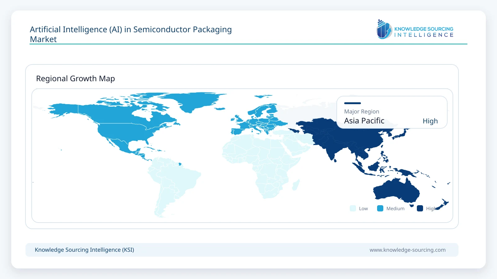
Asia Pacific is the largest deployment region for AI in semiconductor packaging because it contains the majority of global outsourced semiconductor assembly and test capacity together with leading foundries, memory suppliers, substrate manufacturers and advanced-packaging production lines. Taiwan, South Korea, China, Japan, Malaysia and Singapore collectively operate a dense packaging ecosystem where improvements in inspection throughput, yield learning and equipment utilization can be applied across very large production volumes.
Advanced packaging intensifies this opportunity. Taiwan is central to 2.5D and chiplet integration through TSMC and ASE, while South Korea combines HBM manufacturing with advanced packaging investment from Samsung Electronics and SK hynix. China has a large OSAT base and is expanding domestic semiconductor manufacturing analytics, while Malaysia and Singapore continue to attract packaging, test and equipment investment. AI-based inspection and manufacturing analytics can therefore scale across both leading-edge AI packages and higher-volume conventional assembly operations.
The region is also becoming an important software and smart-factory deployment market. ASMPT is headquartered in Singapore and is combining advanced packaging with intelligent factory technologies. Onto Innovation, KLA, Applied Materials, Camtek and other process-control suppliers maintain large installed bases across Asian packaging customers. The near-term market is therefore led by inspection and yield analytics, while agentic design and cross-factory data orchestration grow as manufacturers standardize data models and connect package-design intent with production results.
North America leads development of AI-enabled electronic design automation and semiconductor analytics through Cadence, Synopsys, Siemens EDA, KLA, Onto Innovation and PDF Solutions. Europe contributes through Siemens EDA, Besi and advanced equipment development, while the Middle East and other regions remain smaller demand markets with activity concentrated in emerging semiconductor manufacturing and research programs.
Competitive Landscape
The competitive landscape spans three overlapping groups: electronic design automation suppliers, process-control and inspection companies, and semiconductor manufacturing analytics platforms. Cadence, Synopsys and Siemens EDA are extending AI from chip design into package planning, routing and multiphysics optimization. KLA and Onto Innovation have mature AI-enabled defect classification and inspection workflows, while PDF Solutions specializes in cross-factory manufacturing analytics, ModelOps and AI-driven yield intelligence.
Equipment suppliers are increasingly adding intelligent control and data integration around physical packaging processes. Applied Materials is expanding advanced-packaging process control, ASMPT combines packaging equipment with intelligent factory infrastructure, and Camtek addresses inspection and metrology for HBM, chiplets and hybrid bonding. Besi, Kulicke & Soffa, Advantest, Teradyne and Nordson participate through bonding, assembly, test and inspection environments where AI can improve process stability or quality decisions.
Competitive advantage depends less on access to generic AI models than on semiconductor-specific data, integration with production tools and the ability to validate recommendations against physical process constraints. Vendors with installed equipment bases can embed AI directly at the tool edge, while analytics platforms compete on cross-tool data normalization and model deployment. EDA suppliers differentiate through physics-aware optimization and the ability to keep AI-generated decisions inside signoff-qualified design environments.
Major companies and ecosystem participants covered: Cadence Design Systems, Synopsys, Siemens EDA, KLA, Onto Innovation, PDF Solutions, Applied Materials, ASMPT, Camtek, Kulicke & Soffa, Besi, Advantest, Teradyne, Cognex and Nordson.
Recent Developments
September 2026: Synopsys and TSMC expanded collaboration around agentic AI, AI-powered design flows and advanced multi-die packaging methodologies.
September 2026: PDF Solutions introduced Exensio Aurora, designed to support petabyte-scale semiconductor analytics and secure agentic AI across manufacturing operations and the supply chain.
July 2026: Cadence introduced AuraStack AI Super Agent for advanced packaging and PCB design, coordinating specialized AI agents across planning, implementation and multiphysics analysis.
July 2026: Synopsys and Intel Foundry expanded certified AI-powered EDA and multiphysics flows for Intel 14A and advanced EMIB/EMIB-T multi-die packaging.
May 2026: Onto Innovation presented a multi-stage AI-driven inspection workflow reporting a 95% reduction in nuisance defects and 100% wafer-pattern classification accuracy.
April 2026: ASMPT highlighted the integration of advanced semiconductor packaging, intelligent assembly and factory-level information flow at SEMICON Southeast Asia 2026.
AI in Semiconductor Packaging Market Scope:
| Report Metric | Details |
|---|---|
| Total Market Size in 2026 | USD 1.45 billion |
| Total Market Size in 2032 | USD 6.03 billion |
| Forecast Unit | USD Billion |
| Growth Rate | 26.8% |
| Study Period | 2021 to 2032 |
| Historical Data | 2021 to 2024 |
| Base Year | 2025 |
| Forecast Period | 2026 – 2032 |
| Segmentation | Application, Packaging Process, AI Technology, Deployment Layer |
| Companies |
|
Market Segmentation
By Application
Inspection and Defect Classification
Yield and Root-Cause Analytics
Package Design and Multiphysics Optimization
Process Control and Recipe Optimization
Predictive Maintenance and Equipment Analytics
Data Feed-Forward and Predictive Test
By Packaging Process
Wafer-Level and Fan-Out Packaging
2.5D Interposer and Bridge Integration
3D Stacking and Hybrid Bonding
HBM Assembly and Test
Panel-Level Packaging
Conventional Assembly and Final Package Inspection
By AI Technology
Machine Learning and Predictive Analytics
Deep Learning and Computer Vision
Generative and Agentic AI
Digital Twins and Physics-Informed AI
By Deployment Layer
Package Design and Engineering
Inspection and Metrology Tools
Assembly and Bonding Equipment
Manufacturing Analytics Platforms
Test and Quality Operations
By Customer Type
Foundries
Outsourced Semiconductor Assembly and Test Providers
Integrated Device Manufacturers
Memory Manufacturers
Fabless and System Semiconductor Companies
By Region
Asia Pacific
Taiwan
South Korea
China
Japan
Southeast Asia
North America
Europe
Rest of World
Table of Contents
1. EXECUTIVE SUMMARY
1.1. Market Opportunity and Key Findings
1.2. AI Adoption across Semiconductor Packaging
1.3. Principal Revenue Pools
2. MARKET OVERVIEW
2.1. AI in Packaging Design and Manufacturing
2.2. Inspection, Metrology and Defect Classification
2.3. Yield Analytics and Root-Cause Identification
2.4. AI-Assisted Package Design and Multiphysics
2.5. Factory Data Integration and Model Deployment
3. MARKET SIZE AND FORECAST, 2026-2032
3.1. Global Market Revenue
3.2. Annual Growth Analysis
3.3. Software, AI-Enabled Equipment Functionality and Services
4. MARKET BY APPLICATION
4.1. Inspection and Defect Classification
4.2. Yield and Root-Cause Analytics
4.3. Package Design and Multiphysics Optimization
4.4. Process Control and Recipe Optimization
4.5. Predictive Maintenance and Equipment Analytics
4.6. Data Feed-Forward and Predictive Test
5. MARKET BY PACKAGING PROCESS
5.1. Wafer-Level and Fan-Out Packaging
5.2. 2.5D Interposer and Bridge Integration
5.3. 3D Stacking and Hybrid Bonding
5.4. HBM Assembly and Test
5.5. Panel-Level Packaging
5.6. Conventional Assembly and Final Package Inspection
6. MARKET BY AI TECHNOLOGY
6.1. Machine Learning and Predictive Analytics
6.2. Deep Learning and Computer Vision
6.3. Generative and Agentic AI
6.4. Digital Twins and Physics-Informed AI
7. MARKET BY DEPLOYMENT LAYER
7.1. Package Design and Engineering
7.2. Inspection and Metrology Tools
7.3. Assembly and Bonding Equipment
7.4. Manufacturing Analytics Platforms
7.5. Test and Quality Operations
8. MARKET BY CUSTOMER TYPE
8.1. Foundries
8.2. Outsourced Semiconductor Assembly and Test Providers
8.3. Integrated Device Manufacturers
8.4. Memory Manufacturers
8.5. Fabless and System Semiconductor Companies
9. REGIONAL MARKET
9.1. Asia Pacific
9.1.1. Taiwan
9.1.2. South Korea
9.1.3. China
9.1.4. Japan
9.1.5. Southeast Asia
9.2. North America
9.3. Europe
9.4. Rest of World
10. MARKET DYNAMICS
10.1. Drivers
10.1.1. Advanced Packaging Process Complexity
10.1.2. Growth in Packaging Data Volume
10.1.3. AI-Assisted Multiphysics and Package Design
10.1.4. Chiplet Data Continuity across Distributed Supply Chains
10.2. Restraints
10.2.1. Fragmented Data and Equipment Interfaces
10.2.2. Model Drift and Explainability Requirements
10.2.3. Semiconductor IP and Data-Security Constraints
10.2.4. Integration Cost across Legacy Factory Systems
11. COMPETITIVE LANDSCAPE
11.1. Market Structure and Competitive Intensity
11.2. AI-Enabled EDA and Package-Design Positioning
11.3. Inspection, Defect Classification and Process-Control Platforms
11.4. Manufacturing Analytics and Factory-Level AI Integration
11.5. Foundry, OSAT and Equipment Ecosystem Partnerships
12. COMPANY PROFILES
12.1. Cadence Design Systems
12.2. Synopsys
12.3. Siemens EDA
12.4. KLA
12.5. Onto Innovation
12.6. PDF Solutions
12.7. Applied Materials
12.8. ASMPT
12.9. Camtek
12.10. Kulicke & Soffa
12.11. Besi
12.12. Advantest
12.13. Teradyne
12.14. Cognex
12.15. Nordson
13. RECENT DEVELOPMENTS
14. APPENDIX
Navigate
Trusted by the world's leading organizations











