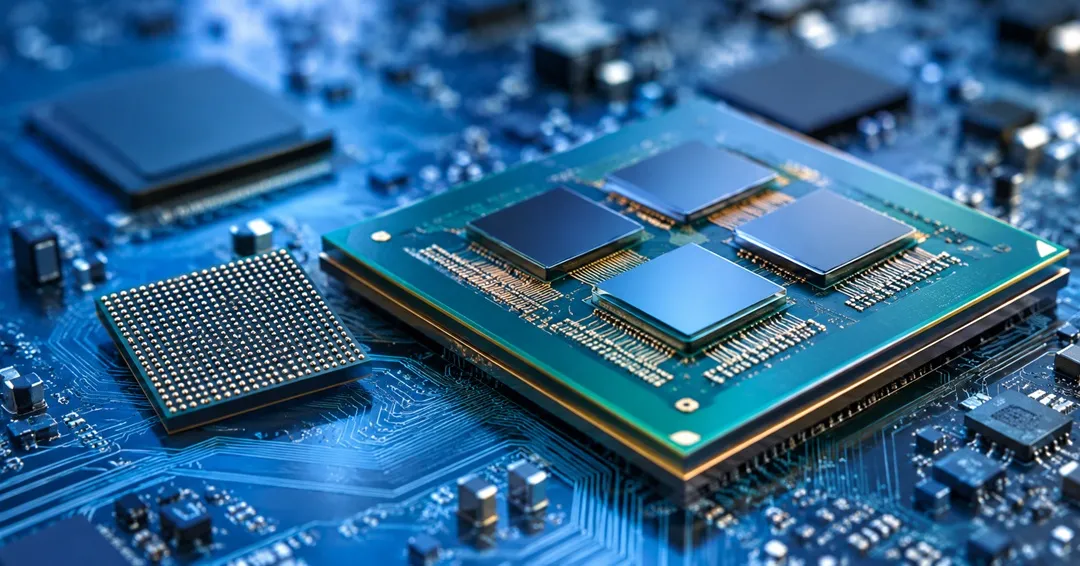
The global chiplet market is expanding as demand for AI accelerators, high-performance computing, and scalable semiconductor architectures increases. Advances in 2.5D integration, 3D stacking, and standardized die-to-die interconnects are accelerating adoption. Semiconductor companies are focusing on heterogeneous integration, manufacturing efficiency, and high-bandwidth connectivity to improve computing performance.
Knowledge Sourcing Intelligence (KSI) projects the global chiplet market to grow from USD 32.0 billion in 2026 to USD 109.9 billion by 2032, registering a compound annual growth rate (CAGR) of 22.8%. Increasing demand for artificial intelligence (AI) accelerators and high-performance computing (HPC), alongside advances in semiconductor packaging, is accelerating the adoption of chiplet-based architectures. As conventional monolithic chip designs encounter growing challenges related to manufacturing complexity, die size, and performance scaling, semiconductor manufacturers are increasingly adopting multi-die integration to develop more flexible and scalable computing platforms.
Chiplets integrate multiple specialized semiconductor dies within a single package, allowing manufacturers to combine computing, input/output (I/O), memory-related, and control functions using different process technologies. This architecture provides greater design flexibility, supports the reuse of semiconductor components, and enables manufacturers to optimize individual dies according to their functional requirements. Its commercial relevance is increasing as processor developers seek to improve computing density without relying entirely on increasingly complex monolithic designs.
Expanding AI infrastructure is strengthening demand for processors capable of delivering higher computing performance, memory bandwidth, and energy efficiency. Advanced packaging technologies, including 2.5D integration and 3D stacking, are enabling high-density connections between multiple semiconductor dies. However, complex packaging requirements, thermal management, manufacturing yields, testing procedures, and inter-die communication remain important challenges affecting large-scale commercialization.
Request a free sample copy or view the report summary: Chiplet Market Report
Key Growth Drivers
Growing Demand for AI Accelerators
AI training and inference workloads require substantial processing capacity, high memory bandwidth, and efficient data movement between computing components. Chiplet architectures allow semiconductor manufacturers to integrate specialized compute and I/O dies within scalable processor packages, supporting increasingly complex accelerator designs. AMD's Instinct MI350X and MI355X accelerators, featuring eight accelerator complex dies (XCDs) and two I/O dies (IODs) connected through Infinity Fabric technology, demonstrate the commercial application of multi-die integration in advanced AI computing. The MI350P uses a smaller configuration of four XCDs and one IOD, illustrating how chiplet-based architectures can accommodate different product requirements.
Advancements in Semiconductor Packaging
Developments in advanced packaging are improving the feasibility of integrating multiple semiconductor dies within a compact package. TSMC's Chip-on-Wafer-on-Substrate (CoWoS) and System on Integrated Chips (SoIC), alongside Intel's Embedded Multi-die Interconnect Bridge (EMIB) and Foveros platforms, support different approaches to heterogeneous integration and die-to-die connectivity. These technologies enable manufacturers to combine computing, memory, and other semiconductor functions while optimizing performance, footprint, and power consumption. Broadcom's 3.5D eXtreme Dimension System in Package (XDSiP) platform further demonstrates the development of advanced multi-dimensional integration for custom AI processors.
Advanced packaging is an important enabler of chiplet adoption but represents a distinct segment of the semiconductor value chain. KSI's chiplet market estimates distinguish chiplet-related products and solutions from standalone assembly services, interposers, substrates, and manufacturing-equipment revenues.
Manufacturing Efficiency and Design Flexibility
Chiplets allow designers to manufacture different semiconductor functions using process nodes suited to their individual requirements instead of placing every component on the most advanced technology. Separating compute, I/O, and control functions can improve silicon utilization and support the reuse of established designs across product generations. This approach also provides opportunities to develop customized processors for AI, networking, automotive, and data center applications. However, the economic benefits depend on production volumes, packaging complexity, manufacturing yields, and integration requirements.
Standardization of Die-to-Die Interconnects
Universal Chiplet Interconnect Express (UCIe) is supporting the development of standardized communication between compatible semiconductor dies. The UCIe 3.0 specification introduced data rates of up to 64 GT/s, improving the bandwidth available for communication across chiplet-based systems. In November 2026, the UCIe Consortium released version 4.0, extending the standard with on-package memory connectivity, improved bandwidth density, enhanced power efficiency, and additional security and system-management capabilities. The introduction of standardized memory connectivity is particularly relevant to AI and HPC systems, where data movement and memory bandwidth are becoming increasingly important performance considerations. Wider adoption of interoperable standards could encourage participation from semiconductor IP developers, fabless companies, foundries, and specialized technology providers.
Latest Industry Developments
November 2026 – UCIe Consortium Releases Version 4.0: The UCIe Consortium introduced its fourth-generation interconnect specification, adding standardized connectivity between system-on-chip devices and memory logic dies. The update also strengthens interconnect efficiency, security, chiplet-state monitoring, and system-level manageability, supporting the development of more interoperable multi-die semiconductor platforms.
September 2026 – Arteris FlexGen Multi-Die: Arteris expanded its multi-die portfolio with FlexGen Multi-Die, addressing data movement and quality-of-service requirements across chip boundaries. The solution targets semiconductor designs for AI, HPC, and consumer electronics as manufacturers transition toward more modular chip architectures.
July 2026 – TYLsemi's Full-Stack Chiplet Platform: TYLsemi emerged from stealth with a USD 43 million funding round to develop a full-stack chiplet platform. Its technology roadmap focuses on connectivity, power delivery, and memory chiplets designed to support customized AI processors and advanced semiconductor integration.
May 2026 – CoAsia Semi's CoCs Platform: CoAsia Semi unveiled its CoAsia Chiplet Solution (CoCs) platform and advanced-packaging roadmap at Samsung Foundry's SAFE Forum 2026. The initiative targets AI and HPC semiconductor applications, with an emphasis on performance, manufacturing yield, and power efficiency.
February 2026 – Broadcom's 3.5D Chiplet-Based Compute Platform: Broadcom announced that it had begun shipping a 2nm custom compute system-on-chip built on its 3.5D XDSiP platform. Developed for Fujitsu, the technology combines 2.5D integration and 3D face-to-face stacking to support scalable, high-performance computing architectures for demanding AI workloads.
Market Segmentation and Regional Outlook
The global chiplet market is segmented by chiplet function, integration architecture, interconnect approach, application, provider type, and geography. Chiplet functions include computing, memory-related, I/O, and other specialized functions, while integration architectures cover 2D multi-chip modules, 2.5D integration, 3D stacking, and hybrid configurations. Interconnect technologies and standards form another important dimension, reflecting the growing requirement for reliable, high-bandwidth communication between semiconductor dies.
Applications span data center CPUs, AI accelerators, custom XPUs, client computing, networking, automotive electronics, and industrial systems. Data center and AI-related applications are becoming important areas of adoption as computing workloads increase the need for scalable processor architectures. Automotive and industrial applications also present opportunities for chiplet integration, particularly where heterogeneous computing and functional specialization can support application-specific requirements.
North America remains a leading region for chiplet design and commercialization, supported by established semiconductor developers, custom silicon initiatives, and sustained investment in AI infrastructure. The presence of major processor designers and semiconductor IP companies strengthens the region's position in chiplet architecture development.
Asia Pacific plays a significant role in chiplet manufacturing and advanced packaging integration. Taiwan, South Korea, China, and Japan contribute through semiconductor foundries, memory manufacturers, packaging providers, and component suppliers. Continued investment in advanced packaging capabilities and semiconductor manufacturing infrastructure is supporting the region's participation in the evolving chiplet ecosystem.
Europe contributes through automotive electronics, industrial computing, semiconductor research, and specialized processor development. Demand for application-specific semiconductor solutions and investment in regional semiconductor capabilities are supporting the development of heterogeneous integration technologies.
Competitive Landscape
The chiplet market includes semiconductor developers, foundries, advanced packaging providers, and semiconductor intellectual property (IP) companies. Major semiconductor developers include AMD, Intel, NVIDIA, Broadcom, and Marvell Technology, although their chiplet architectures, product portfolios, and commercial exposure differ.
The manufacturing and packaging ecosystem includes TSMC and Samsung Electronics in semiconductor fabrication, alongside ASE Technology Holding and Amkor Technology in advanced packaging and assembly. Arm, Synopsys, and Cadence Design Systems contribute through processor IP, semiconductor design software, verification, and implementation technologies.
Competition is increasingly shaped by computing performance, interconnect bandwidth, power efficiency, manufacturing yields, and the ability to integrate dies from different process technologies. Standardized interfaces and collaboration across the semiconductor value chain are becoming important for improving compatibility and supporting commercial scalability. As chiplet architectures become more sophisticated, manufacturers will need to balance performance improvements against packaging costs, thermal constraints, and system-level integration requirements.
Analyst Perspective
"Growing AI infrastructure requirements are strengthening the commercial case for chiplet architectures. Advanced packaging and heterogeneous integration are giving semiconductor manufacturers greater flexibility to scale computing performance and develop application-specific processors. The release of newer interconnect standards is also supporting the evolution of a more interoperable chiplet ecosystem. However, sustained adoption will depend on manufacturing yields, interconnect efficiency, thermal management, and the economics of complex multi-die systems."
What the Study Covers
The report provides a comprehensive assessment of the global chiplet market, including market estimates and forecasts through 2032, growth drivers, restraints, technological developments, and competitive dynamics. It examines chiplet functions, integration architectures, interconnect technologies, application areas, provider categories, and regional market opportunities. The study also evaluates the strategies and capabilities of key industry participants, profiles major companies across the semiconductor ecosystem, and examines relevant industry developments shaping the adoption of chiplet-based architectures.
Have questions?
More Press Releases
Data Center Silicon Photonics Market to Reach USD 23.1 Billion by 2032, Driven by AI Infrastructure and Co-Packaged Optics Adoption
The global data center silicon photonics market is expanding as AI infrastructure, hyperscale computing, and high-bandwidth networking increase demand for advanced optical connectivity. Innovations in co-packaged optics, photonic integrated circuits, and energy-efficient interconnects are creating growth opportunities, while manufacturing scalability, thermal management, and integration costs remain important industry considerations.
Global Automotive Thermal Comfort Systems Market to Reach USD 22.5 Billion by 2031, Driven by Heat Pump Adoption in Electric Vehicles
The global automotive thermal comfort systems market is projected to reach USD 22.5 billion by 2031, driven by electric vehicle adoption, heat pump integration, and energy-efficient cabin heating. Advances in integrated thermal management, localized heating, and intelligent climate control are creating opportunities for automotive suppliers worldwide.
Liquid Air Energy Storage Market to Reach USD 2.25 Billion by 2032 as Commercial-Scale Projects Gain Momentum
The global liquid air energy storage market is gaining momentum as renewable energy integration and long-duration electricity storage requirements drive investment. Commercial-scale project development, cryogenic technology advancements, thermal integration, and grid-stability applications are creating new opportunities, while project financing, capital costs, and operational efficiency remain important considerations for market expansion.